
Audio ADC with superb performance figures in a compact form factor. Suits audio recording kit, Hifi systems, or audio measurement applications.
- Up to 768 kHz / 32-bit audio
- Very high (measured) performance, typically:
- 121 dBA dynamic range / SNR (124 dBA in mono mode)
- -113 dB THD+N (-1 dBFS, 1 kHz)
- -117 dB THD (-8 dBFS, 1 kHz)
- -130 dB crosstalk (10 kHz)
- Balanced differential input
- Stereo or mono operation
- I2S output; Master or Slave
- HW configurable (supports I2C as well)
- Assembled boards available
Introduction
This ADC is suitable for audio recording kit or hifi audio use; for example, connecting a turntable or other analog source in a DSP system. Another use and where this was originally designed for is DIY audio measurement setup. Paired with a connection to PC and appropriate PC software, one can create a very capable low cost audio analyzer setup.
Outstanding performance figures mean this ADC does not need to be embarrassed beside any ADC; not saying it is the best of the best but certainly a top shelf product in terms of technical performance.
As something new, I have also made a video about this board. It briefly goes through the board with features, connections, schematics, and measurements. There is also a 2-page factsheet to provide key information without reading this whole post.
Design
See schematics PDF at bottom of the page or schematics walkthrough in the video above.
Input circuit consists of simple high-pass and low-pass filtering and input protection, followed by buffers and finally differential amplifier for pre-ADC low-pass filtering and also biasing the input at half-rail.
There is some level of input protection but it is not really suitable for robust measurement setup as is. One should add something to limit current in case of overvoltage at the input. In normal Hifi or recording ADC application this does not matter but in a lab measurement kit prone to abuse it does. There is a combination of diodes and zeners that clamp the input voltage just about at the maximum rating of ADC input. However, these small diodes cannot withstand significant current for long period of time in case of a continuous overvoltage state (and capacitance of larger diodes caused THD degradation at higher frequencies). In such situation something should sense the state and cut the input. Or alternatively, as is often used in commercial audio analysers, use light bulbs which inherently behave as nonlinear resistors.
Power supply is fairly basic considering the performance of the unit. ADP7118 regulator is a low noise LDO but nothing extreme. It works very well in this application though. Voltage reference of AK5572 is not even nearly as picky as the ones found in AK4490 and AK4493 DACs I’ve had quite some challenges with. 10R and 1000u in the reference pin does a good job getting a clean reference without affecting THD.
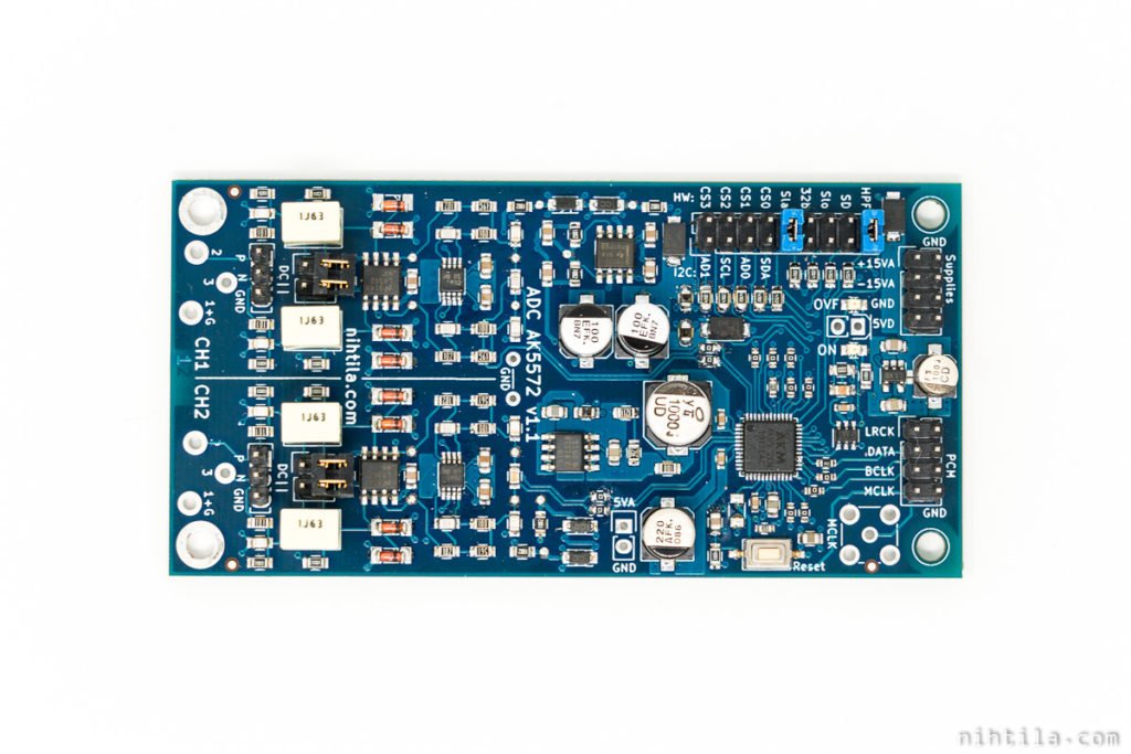
Connectors
There are no audio connectors on board by default as it was originally designed for audio measurement application with some sort of input scaler circuit before the ADC; I have not designed such circuit yet. However, there are placeholders for XLR connectors; they come slightly out of the board though. Obviously one can wire out connectors as well. XLR’s can be wired directly using the 3 pins provided but even for single-ended application it is recommended to use XLR connectors at this end and use RCA to XLR cable.
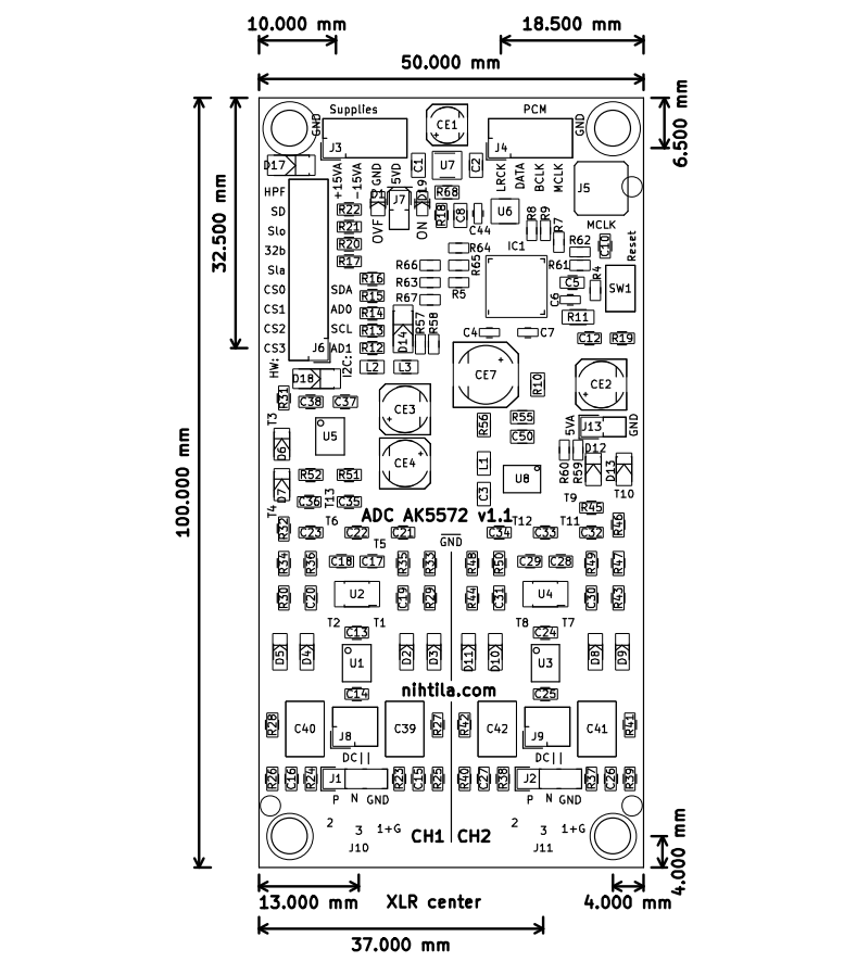
Power supply connectors are just pinheaders as opposed to screw terminals. This is also partly due to the original design being for measurement application but also to keep the board at 50x100mm – the price of 4-layer boards tend to increase significantly when going larger than this. 4-layers is an absolute must for a circuit like this and careful layout plays a crucial role in getting the maximum performance.
Components
Used components are very high quality parts intended for audio applications. ADC is AKM AK5572. Opamps are LM4562 and OPA1632 for input circuit and NE5532 for bias buffer. All capacitors in signal path are film or C0G types and resistors are 0.5% thin film type.
PCB
Layout is a carefully designed 4-layer 50mm x 100mm design.
As usually, schematics and layout have been done with KiCad and PCBs ordered from Elecrow. Components are sourced from Mouser and Digikey. Boards have been assembled using my DIY reflow oven.
Configurations and settings
By default the ADC chip is in parallel/hardware mode and jumper links in 2×9 pinheader change settings such as clocking, sample rate, master/slave and so on. These settings are described below. Also, 0R links are used throughout setting pins so it is possible to cut these links and add jumper wires to change some settings not accessible by the jumper links.
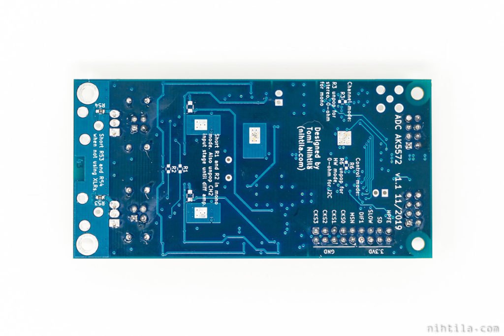
As opposed to hardware mode, the chip can be set to I2C mode by placing a resistor on the bottom side of the PCB. Then SCL and SDA are available at the pinheader for software configuration with Arduino or similar.
Clock configration
Jumpers CS0-CS3 configure clocks. See full table in AK5572 datasheet; however, the most important values are shown below. Sample rate depends on Master Clock and 24.576 MHz is assumed here.
It’s difficult to give default or recommended sample rate as it depends on the system. However, I would consider 192 kHz a good default with 24.576 MHz Master Clock. That’s how all measurements have been done. It gives basically identical superb audio performance as 48 kHz but you get benefits of higher bandwidth as seen in digital filter square wave measurements.
| CS3 | CS2 | CS1 | CS0 | Sample rate |
| open | close | close | open | 768 kHz |
| open | close | close | close | 384 kHz |
| close | close | close | close | 192 kHz |
| close | close | open | open | 96 kHz |
| close | open | open | close | 48 kHz |
Digital filter
This is a setting for internal digital low-pass filter type.
If you do not understand or care about digital filters, just leave the default setting and don’t worry.
| SD | Slo | Filter roll-off type |
| open | open | Sharp (default) |
| open | close | Slow |
| close | open | Short Delay Sharp |
| close | close | Short Delay Slow |
Other settings
Below are the rest of the jumper links.
| Jumper | Open | Close |
| HPF | Digital HPF disabled | HPF enabled (default) |
| 32b | 24-bit I2S data (default) | 32-bit I2S data |
| Sla | ADC is I2S Master | I2S Slave (default) |
| J8 DC | Input 1 AC coupled (default) | DC coupled |
| J9 DC | Input 2 AC coupled (default) | DC coupled |
Reset button is included as AK5572 datasheet says the device should be resetted every time settings are changed. The button makes it a bit easier than power toggle when experimenting with the board.
By default master clock (MCLK) input is in a pinheader but there is also an option to solder SMB connector and 50R resistor for better signal integrity, especially if cable is long. That being said, none of the wires from I2S connector should be long.
Other points:
- Inputs can be AC or DC coupled with a change of jumper link position.
- It’s recommended to keep (digital) HPF in use as there will be quite some DC-offset otherwise.
- There is an LED for power on and input clipping (OVF).
- Logic level is 3.3 V.
Measurements
Measurements have been carried out using Audio Precision APx555 audio analyser. Unless otherwise mentioned, measurement bandwidth is 20 kHz and frequency in single-tone measurements is 1 kHz. The board is powered by a bench PSU.
Given measurements are not guaranteed but typical values; however, performance is expected to be fairly consistent across boards.
Maximum signal level is 3.6 Vrms differential which gives 0 dBFS digital signal.
These measurements have been done at 192 kHz sample rate and using default Sharp filter. Differential input was used but there are some single-ended results at the end as well.
In the ADC5572 video I have explained a bit more about some measurement results.
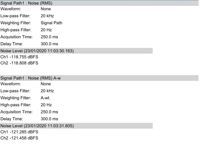
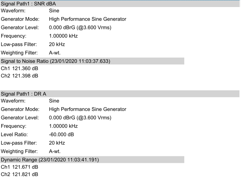
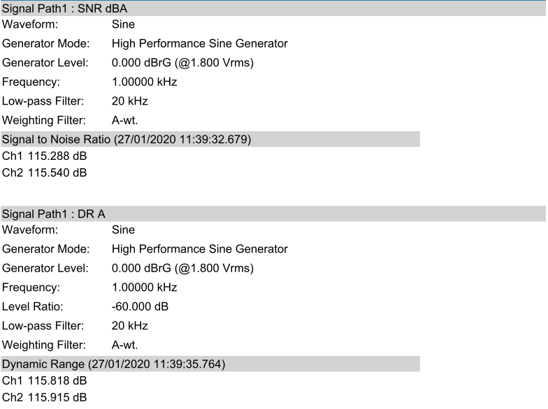
Dynamic range and noise
Unweighted noise is -119 dBFS (and SNR thus the same) and A-weighting increases it to -121 dBFS.
Dynamic range matches SNR at 121 dBA. AK5572 IC spec is also 121 dBA.
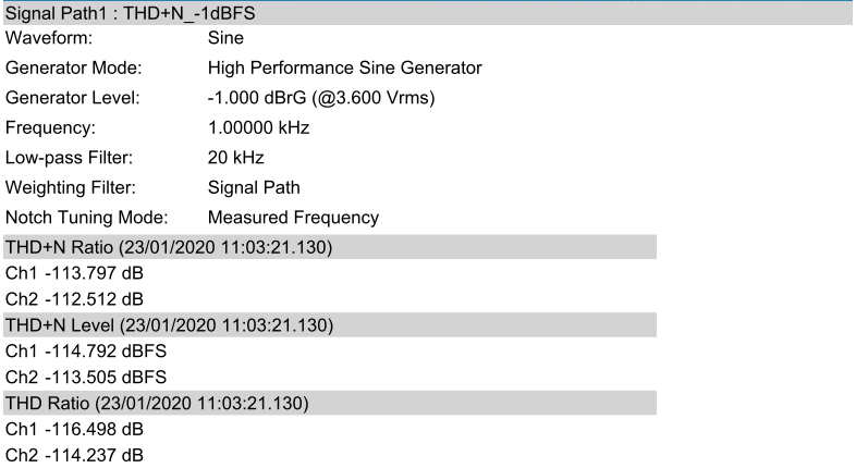
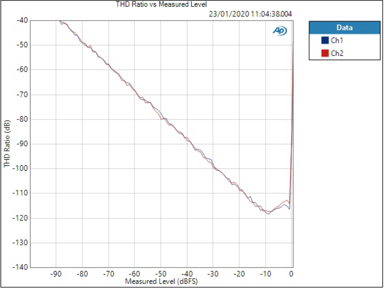
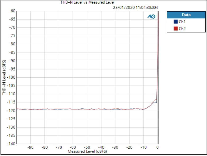
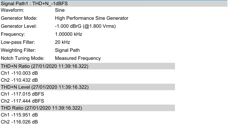
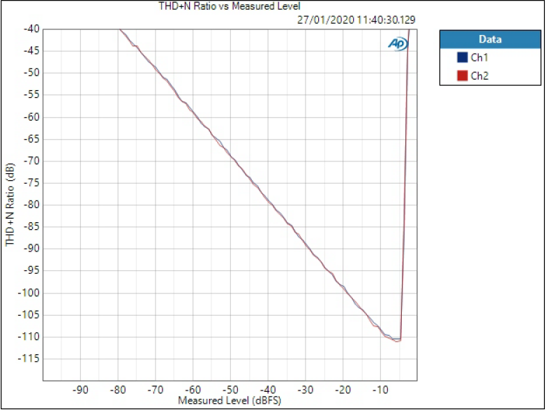
THD+N and THD
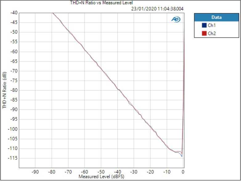
Summary of THD(+N) figures is below. Overall these are impressive results. THD+N figures slightly exceed -112 dB spec.
There is a slight difference between channel 1 and 2 near maximum level. Plots show that these channels are identical until just before maximum level. This has no practical meaning and rarely channel performance is exactly identical; normally you just don’t see such comparison. If identical performance is required in a measurement application, it may be better to use two boards in mono mode.
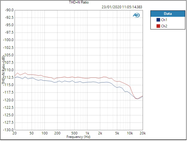
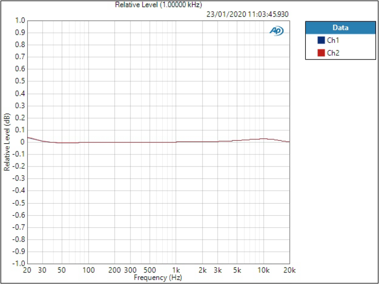
Frequency response, phase, and crosstalk
These are more like sanity checks that everything is correct.
Low frequency roll-off is due to measurement filter and slight deviation at high frequency is due to digital filter. Note the scale though; deviation measured is only 0.023 dB.
Crosstalk is so low that it is basically non-existent. There is no need to go mono mode due to crosstalk.
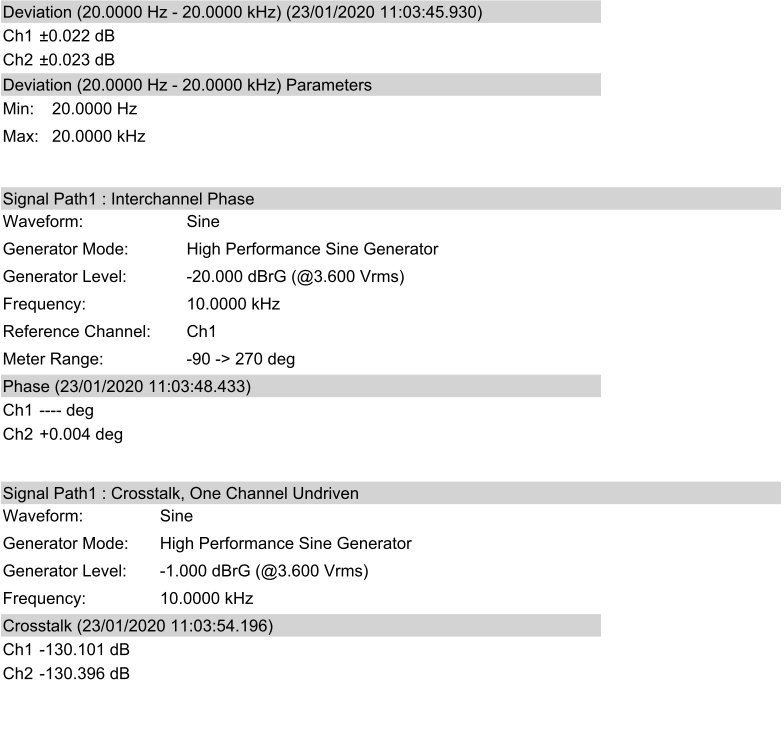
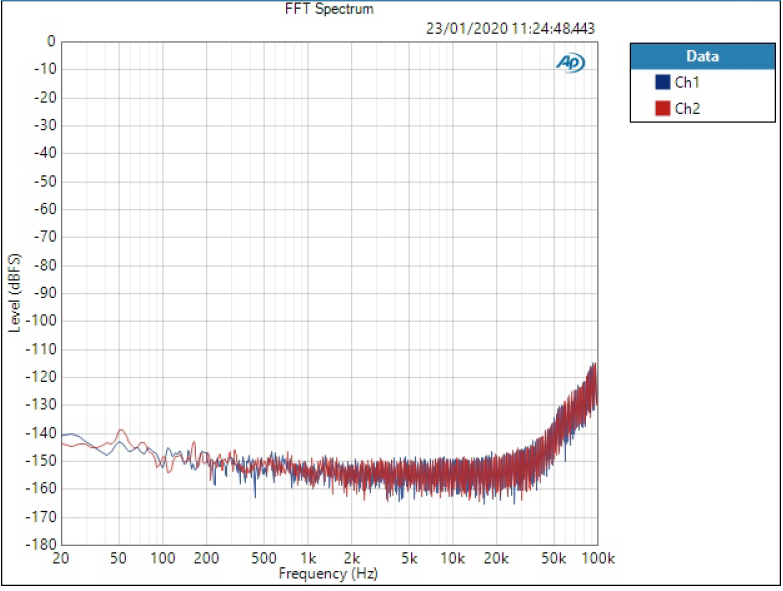
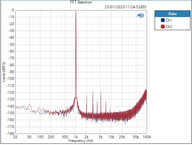
FFTs
There are a couple of FFTs to show spectra. A note here is that noise floor increases quite heavily after audio band due to noise shaping. This has zero meaning in Hifi application but may interest someone doing higher bandwidth audio measurements.
Single-ended measurements
All measurements above are done using differential input. What if we use single-ended input?
The main difference is that we lose 6 dB of signal level and dynamic range. This is simply because in order to get 0 dBFS signal we need 1.8 Vrms signal on both positive and negative input in opposite phase. Going higher causes input signal protection to clip which is somewhat a limitation of this circuit. If single-ended input is the main or only use, one could use a signal inverter for the negative input. However, due to inherently very high dynamic range, even losing 6 dB still gives very impressive figure. If I was to use this in a Hifi system I wouldn’t worry about the lost 6 dB.
If you use this ADC in a Hifi system with unbalanced (RCA) connections, I recommend still using XLRs in this ADC end. Then just use RCA to XLR cable as they should have a separate negative conductor and shield that will still help a bit with noise pickup.
There is no degradation in distortion when using single-ended input.
Power consumption
The board draws significant current to achieve these performance levels. Therefore, it is normal that the PCB becomes relatively warm and opamps hot to touch; thermal camera shows they can reach 70 C. It is not recommended to mount the board in a small completely closed enclosure; some venting is preferred. The whole board dissipates around 3 W so it’s nothing extreme but quite a lot for this sort of board.
Measured power figures at 192 kHz sample rate:
- 5VD: 12mA
- 15VA: 89mA
- -15VA: 62mA
Digital filters
There are four digital filters in AK5572 IC:
- Sharp (default)
- Slow
- Short Delay (SD) Sharp
- Short Delay (SD) Slow
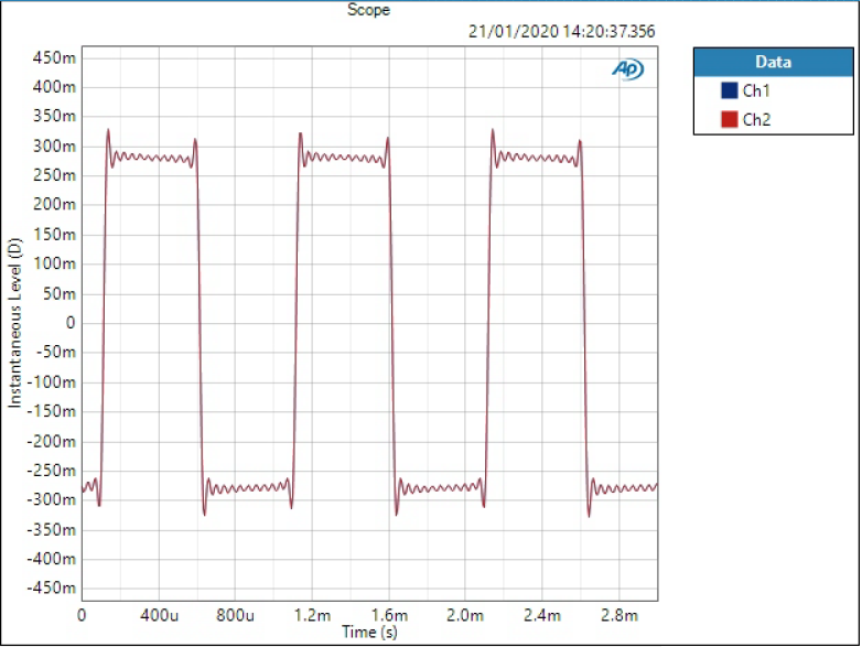
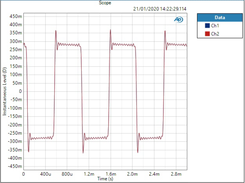
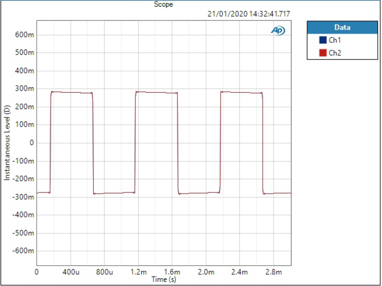
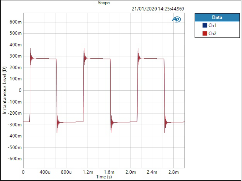
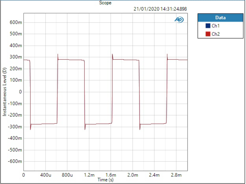
They are documented quite well in AK5572 datasheet. I am not going to analyse the filters in more detail here, just list 1 kHz square wave captures of each filter at 48 kHz and 192 kHz; sample rate plays a big role here. I have written in more detail about DAC digital filters in another post.
If you do not understand or care about digital filters, just leave the default setting and don’t worry.
What we can say from these results is that using 192 kHz sample rate does give some benefits in terms of time-domain response. Thus, it is a good default sample rate if the rest of the system supports it.
1 kHz square wave, 48 kHz sample rate
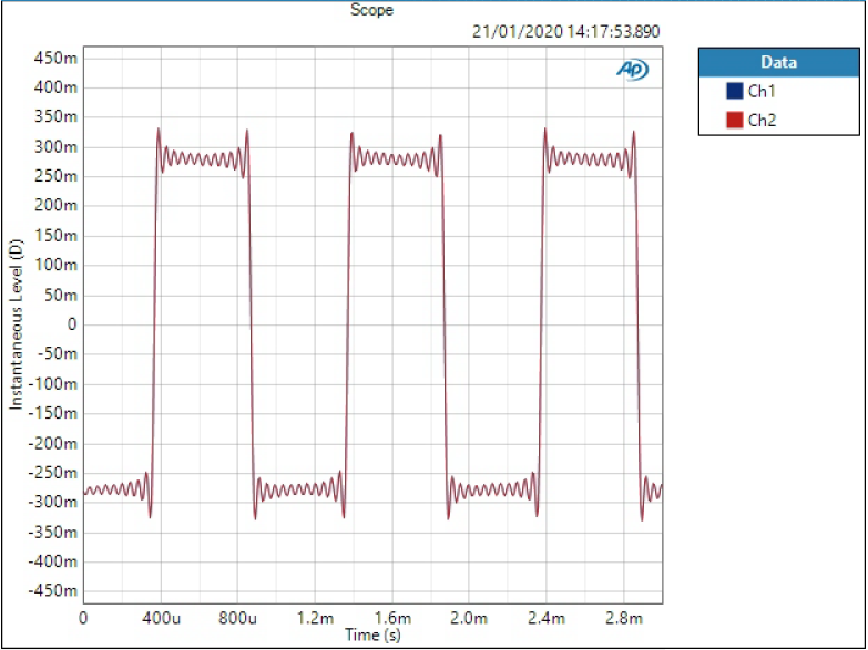
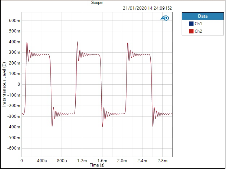
1 kHz square wave, 192 kHz sample rate

Files
References and additional information
There is a compatible I2S to S/PDIF converter available that can even work with two mono ADCs creating one stereo S/PDIF stream.
Version history
Schematics / PCB version history and known errors and bugs
- v1.1A First released version
This page version history
- 2.2.2020 Initial version
Buying instructions here.
9 comments
hey there, nice work !
just a short note: the links under “Files”:
– Component placement top ( https://nihtila.com/wp-content/files/ADC_AK5572_PCBf_meas.pdf )
– Component placement bottom ( https://nihtila.com/wp-content/files/ADC_AK5572_PCBb.pdf )
are “dead” somehow …
Thanks! And thanks for letting me know the broken links, they are fixed now.
Hello Tomi, I am impressed by your design of the ADC AK5572 module, but must admit I am not so technically inclined towards electronics. I actually have DA2USB module bought long ago from beis.de and my question is will ADC AK5572 combined with the DA2USB modules be successful in recording at least 24/96 audio to a PC?
Sorry I have missed your comment, I never got notification. Looks like DA2USB have SPDIF inputs so ADC AK5572 doesn’t work directly with that. I do have SPDIF TX board and with that it would work. I’m not sure if you could make it work by connecting the ADC directly in the middle of the DA2USB, where you split the board. But that would definitely need some more technical understanding and investigation.
I have looked at your SPDIF TX board and what I understood by searches that I made recently, there is DIT chip involved in the design so it will act as some middleman between the ADC and DA2USB module, so it means I shouldn’t have problems connecting the three modules together, i.e. AK5572 ADC -> SPDIF TX -> DA2USB. Am I right?
By the way, I have the instructions how to interconnect the separate modules of the DA2USB as a whole.
Yes, if you use SPDIF in between (between SPDIF TX and DA2USB) then it will work. It’s just that I’m not sure if there was a way to connect it directly using I2S. But at least SPDIF should offer trouble-free way to do it. If there is something you are unsure of or want to discuss more, please send an email using the contact form.
Hello Tomi.
Congratulations about the ADC. For all the reading, measurements, PCB etc.
At first when i saw 768 kHz and 32-bit audio i wanted to jump right into measurements using 768 kHz sample rate. The noise shaping and the available I2S to USB interfaces cooled me down a bit.
I have a question:
What kind of I2S to USB interface can i use with your ADC?
I found https://www.minidsp.com/products/usb-audio-interface/mchstreamer – you wrote about it in your site, but for DAC implementation.
The other, that i saw is :
https://www.diyinhk.com/shop/audio-kits/142-xmos-multichannel-high-quality-usb-tofrom-i2sdsd-spdif-pcb.html#/fifo_option-null/usb_cable-null/xmos_firmware-192k_8ch_out_8ch_in_spdif_out
Best Regards!
Thanks!
You’re right, the noise shaping in AK5572 is very aggressive and starts early which makes measurements at higher sample rates less useful. Unfortunately that is the way to get very low noise within the audio band. Support to those very high sample rates is more like a marketing gimmick in this IC. I may try another IC one day, something with flatter noise above audio band; unfortunately that likely means sacrificing some performance within the audio.
I haven’t tried those I2S to USB modules with this ADC yet, but those are ones with recording support as well so they should work. I shall try MCHStreamer soon as I have it myself. That’s what I plan to use but been busy designing and building some other boards.
Yes. That’s how it is with these ADC DSP techniques. A very good project! I am grabbing a board. 🙂