Updated 18.2.2017
Unfortunately I do not have detailed instructions for each board and I expect potential builder to have relevant electronics skills. If there will be enough interest I may try to write better instructions for more complicated boards.
General instructions
- Good basic electronics skills are expected:
- Good soldering skills
- Use decent soldering iron with small tip. Do not fry components or PCB traces.
- Using flux, either gel, pen, or liquid, makes soldering easier, especially if you need to re-solder something and have old tin in place. Extra flux also makes solder bridges unlikely.
- Ability to recognise components and their polarities, also ensure adequate voltage and current ratings when choosing components yourself. Check pinout if you use some other components than suggested in BOM.
- ESD and electrical safety
- Thermal design – use heatsinks on regulators or mount them on chassis
- When using chassis as heatsink, first tighten individual components and PCB on the chassis and then solder the leads. Tightening screws after components have been soldered causes excess mechanical stress.
- Regulators must be electrically isolated from heatsink/chassis.
- Good soldering skills
- Use provided documents:
- Schematics
- Component placement top and bottom
- At the moment I do not have component reference designators on silk screen on most of the boards so these documents serve that purpose. I will add reference designators in future revisions at least for simpler boards – I just like the tidier look of busy board without extra silk screen information. However, it does make reworking easier.
- PCB images
- BOMs when available; components listed in BOM are the ones used in the prototype but these are not the only options
- Photos are useful to check how components are placed but some values (e.g. resistors) may be incorrect as I may have changed something after taking the photos
- All boards are built and tested and proven to be functional. However, some designs have bugs – check small prints in schematics and board page for extra instructions; the end of each page has a bug list. You will also find board-specific notes at the end of this page.
- It is highly recommended to use lab power supply with current limits when testing boards.
Assembly instructions
- Populate first all power supply components and measure that all voltage rails are correct. You can also do this one supply at a time.
- It can be good to populate all decoupling capacitors at this point as well. If you end up having short circuit between supply and ground it is easier to debug at this point than when all ICs are in place.
- Usually the circuit should not take any current at this point – except the inrush current to charge all capacitors.
- Discharge any big capacitors before moving forward! Or populate some load in the circuit to do that.
- Build boards in blocks and if possible check functionality before moving to next one. It makes debugging easier if something is not working. For example, populate input circuitry and check that signal is coming through. Then move to the next stage and so on.
- Some boards do not have PCB thermals in pads. This can make soldering some components a bit tricky as it takes lots of heat. It may be easier to solder the plane-side pad first. Slightly larger soldering iron tip may be necessary as well. Check carefully that these components are soldered well.
Board-specific notes
Some board specific assembling tips. Read board pages for all extra information and try to understand what is necessary. However, if you have questions when populating boards do not hesitate to ask.
H-DAC
- I have not used thermals on all copper planes. This can make soldering some components a bit tricky as it takes lots of heat. It may be easier to solder the plane-side pad first. Check carefully that these components are soldered well. I will fix that in future revisions and newer designs. Thermals are necessary for convenient soldering and their tiny impact on inductance does not have any meaning in my boards.
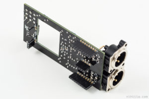
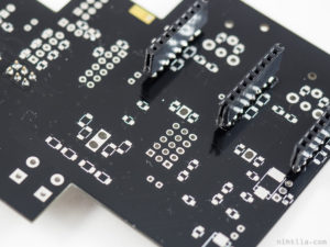
- On-board RCA-connector is slightly taller than normal pinheader. Therefore, when using addon boards, you should use taller pinheaders or solder normal pinheaders/sockets slightly above the board, see photo on the right.
- Do not populate pinheaders P29 and P30, these are only for testing. Short the signals with small wires or 0-ohm resistors.
All H-DAC addons
- H-DAC RCA-connector is slightly taller than normal pinheader. Therefore, when using addon boards, you should use taller pinheaders or solder normal pinheaders (H-DAC) or sockets (addons) slightly above the board, see photo on the right.
Addon H-PreAmp
- LME49724 and TPA6120A2 have thermal pads under the IC. I have used holes in the footprints (see photo) so they can be soldered without hot air station. First solder two opposite top-side pins to keep the component in place, then solder the thermal pad from the bottom side using plenty of heat and solder. By unsoldering one of the pins, make sure the thermal pad is well soldered (part does not move). Solder the rest of the pins.
- It is not necessary to populate P3 and P4 and to take I2S signals from H-DAC to H-PreAmp. This is just an option for future expansion.
- Populate only the required microcontroller circuit components.
- If you want to experiment with balanced headphones connection (requires headphones with separate cabling for each channel), wire grounds separately from P6 and P10 and use 10-ohm series resistors (as are in the headphone outputs).
Smart PSU 3
- Diode silkscreen symbols are wrong way. This happened because pins had been swapped in Kicad version update. Now I have all my components in my own library so it should not happen anymore.
Version history
- 18.2.2017 Initial version

