
I bought a second hand M-DAC to have a well-known commercial reference in terms of measurements and sound. Obviously I needed to open it and see what’s inside. This is not a detailed reverse-engineering report but a glance inside with plenty of photos. Measurements are coming later.
Introduction
Audiolab M-DAC is one of those DACs that caused a lot of buzz among hifi crowds when it was released in 2011. It was highly praised in its price category of around £600 and won awards by What Hi-Fi, Hi-Fi Choice, and EISA. Moreover, at the moment it can be bought new for £470 at Richer Sounds – I got my second hand unit even a lot cheaper off eBay. Anyway, M-DAC is clearly a good reference as it is highly acclaimed in the industry.
M-DAC was designed by John Westlake, a well-known audio designer who has designed electronics for Cambridge Audio, Audiolab, Quad, Pro-Ject, and Creek. I have not been following the threads in Pinkfish media forum where Mr. Westlake has been active but what I understood, he designed the original M-DAC slightly different and obviously more expensive to manufacture, and Audiolab have been understandably cut the corners a bit. Therefore, the more expensive successor M-DAC+ was released few years later. And after that Westlake has been working on his crowdfunded projects.
Something worth mentioning is that John Westlake kept upgrading the firmware of the M-DAC under his own name, or his own company West Lake Audio, after he was not working with Audiolab anymore. There is an M-DAC Wiki page where you can find some information and all the released firmware versions.
Long story short(er), you can find all information on M-DAC online when you just google it. This teardown is not an extensive reverse-engineering or analysis but more like a glimpse what’s inside with lots of photos. After all, an audio engineer is very interested in seeing inside a successful commercial product.
I will also do performance measurements at a later time. Besides basic analog performance measurements, I am also interested in trying to find differences between the several digital filter options M-DAC offers.
Teardown
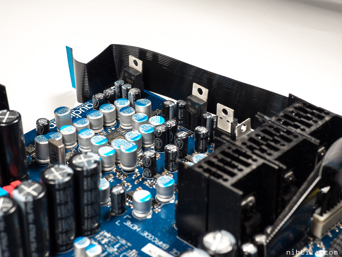
After the case is removed, a pretty busy and large PCB is revealed. The vertical PCB to the left contains some main power supply components. Front panel PCB has been removed and is shown at the end.
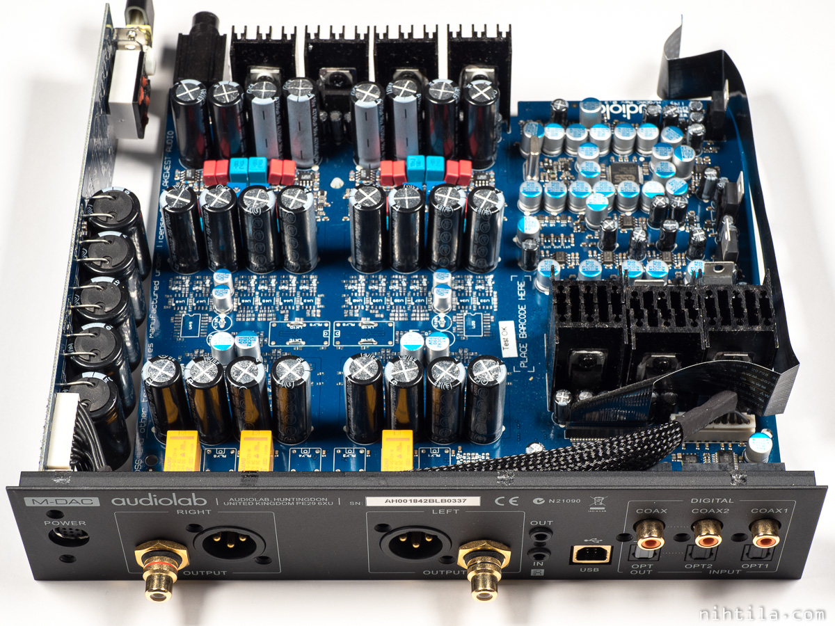
The photo below is uploaded in high resolution so can be zoomed in more.
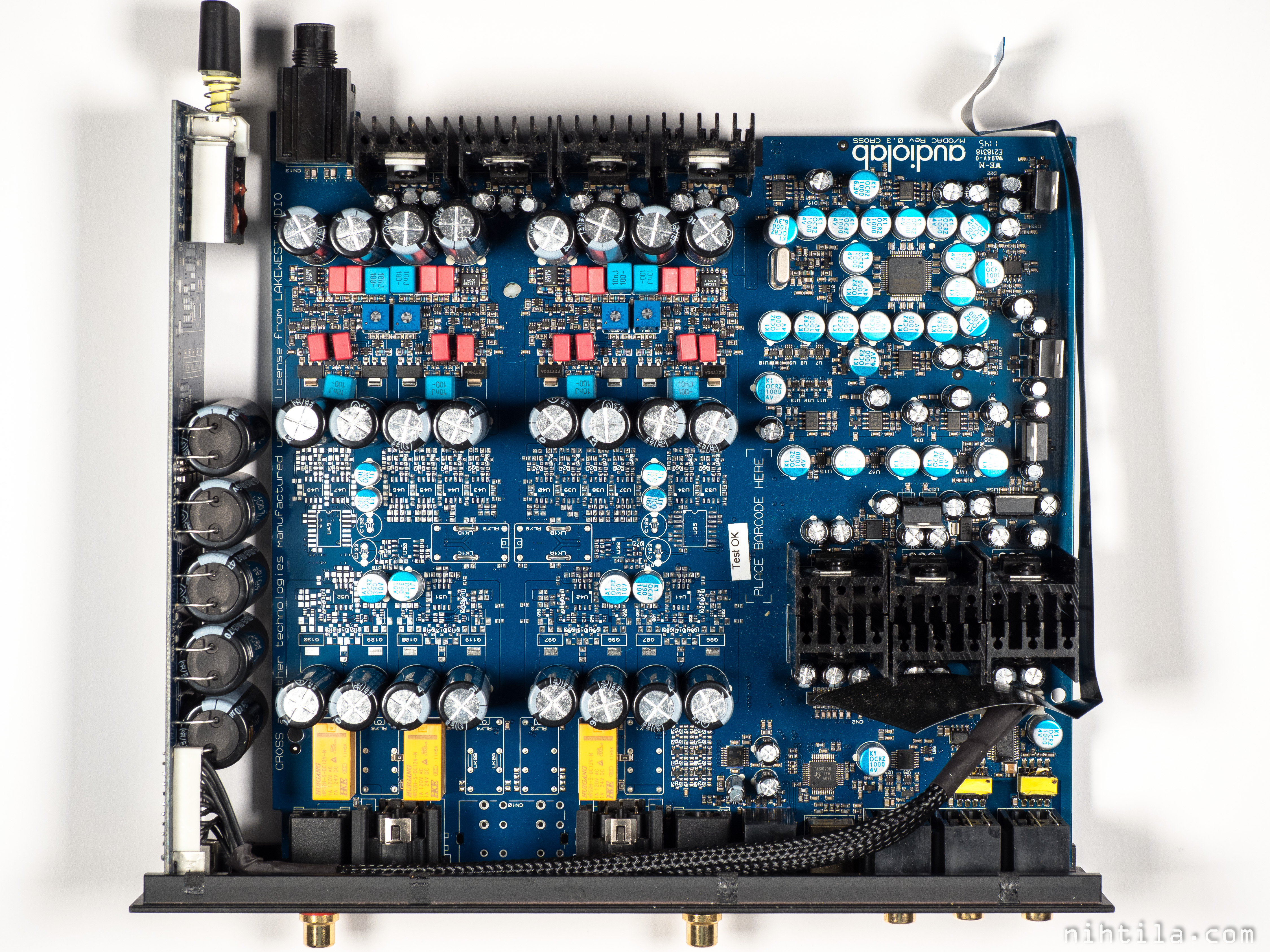
Below is the same photo with some key parts identified. The first impressions were:
- Some serious number of electrolytic capacitors inside!
- There are lots of components unpopulated, wonder what was designed to be there. Even more complicated or additional analog stage? It is located just before the output connectors.
- Many components are quite basic (which I in a way find positive, and to be honest you can’t afford anything exotic at this price point) but there are lots of them, by no means this is a cheap board to manufacture.
Main components:
- ES9018 DAC – very high quality, popular, and famous DAC. Not easy to get as it is not sold by any distributors and you need to contact ESS and sign an NDA to even get the datasheet.
- Wolfson WM8805 S/PDIF receiver
- TI TAS1020B capable of up to 24-bit 96 kHz audio ‘only’, as S/PDIF can work up to 24-bit/192 kHz
- Lots of basic regulators: 7812s and 7912s followed by 317s and 337s
- NE5532 and NE5534 opamps in discrete regulator circuits
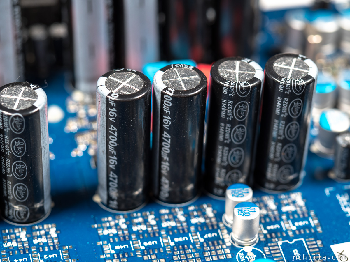
- Loads and loads of electrolytic capacitors and with big values; all those light blue topped SMD electrolytics are 1000 uF and 4 V or 6.3 V; in addition the big 4700 uF through-hole caps which are also plenty
- It seems there are also D-flipflops for reclocking
- Something that looks like a FET-based analog stage
The design philosophy is clearly to engineer an excellent implementation using basic components. And use loads of capacitance everywhere; there must be capacitance worth some decent sized power amplifier. But I like that. No exotics. And based on my initial listening tests this actually sounds really pleasant; although I do not consider myself as ultimate golden-ear. But there is definitely something in this I do not have in my own designs – yet. But that is not really a surprise considering John Westlake’s track record. I need to study this more…
Just a note that you can find some versions of the schematics when you just type it in Google, lacking the analog stage though. And that part probably have a lot to do with the sound quality of this thing. We can see that the components there differ from the rest; there are some different looking resistors, through-hole plastic capacitors, FETs, and trimmer resistors.
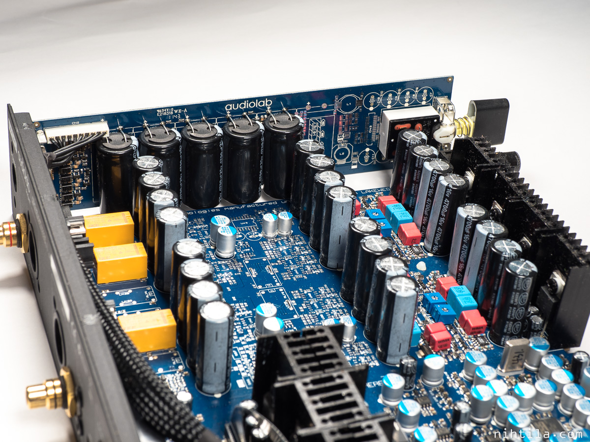
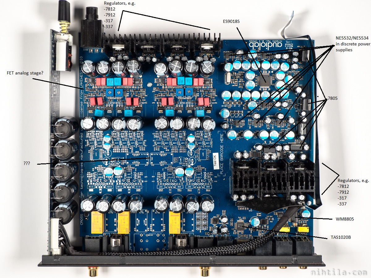
Huge amount of capacitance
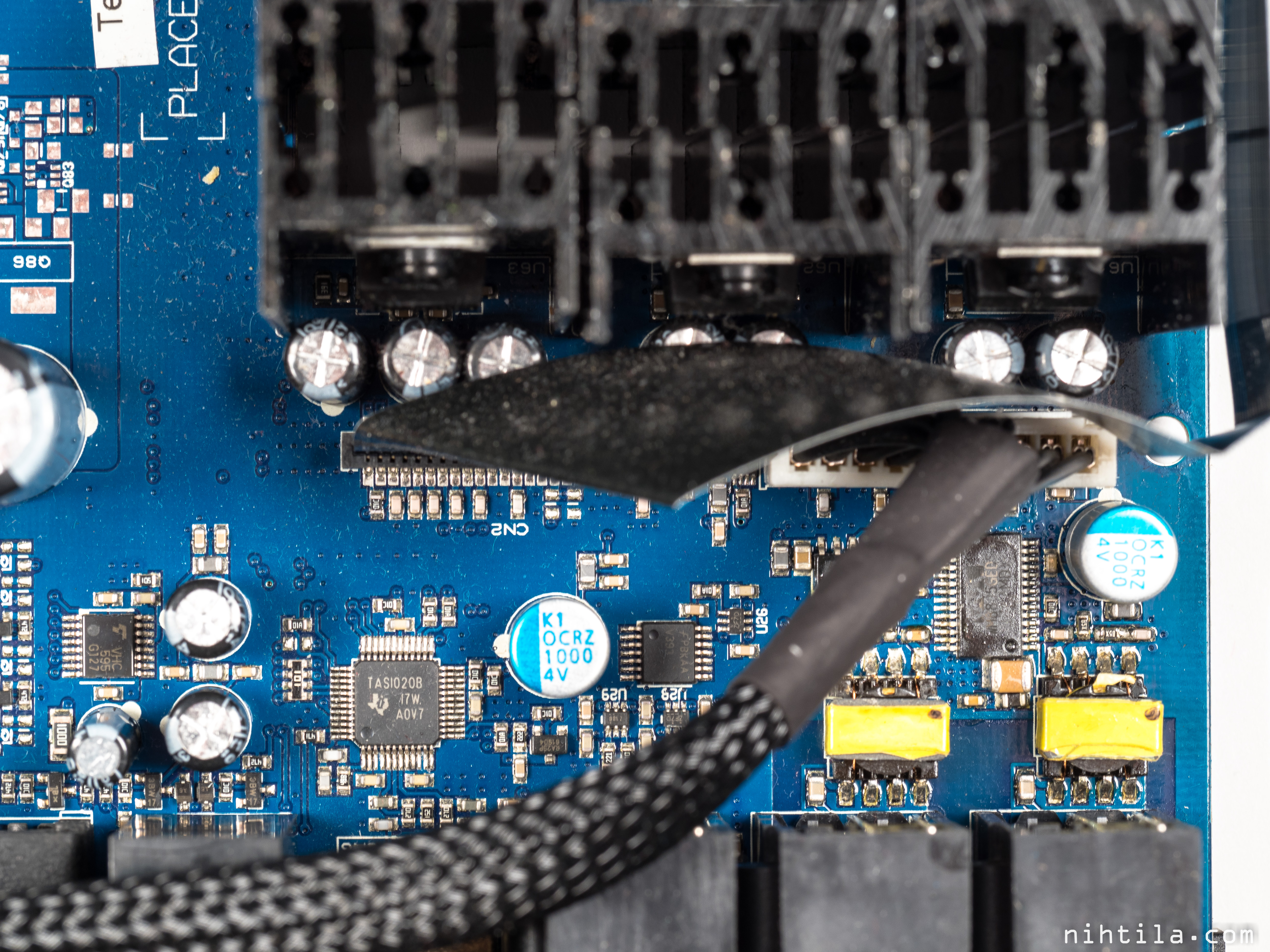
TAS1020B USB receiver and WM8805 S/PDIF receiver
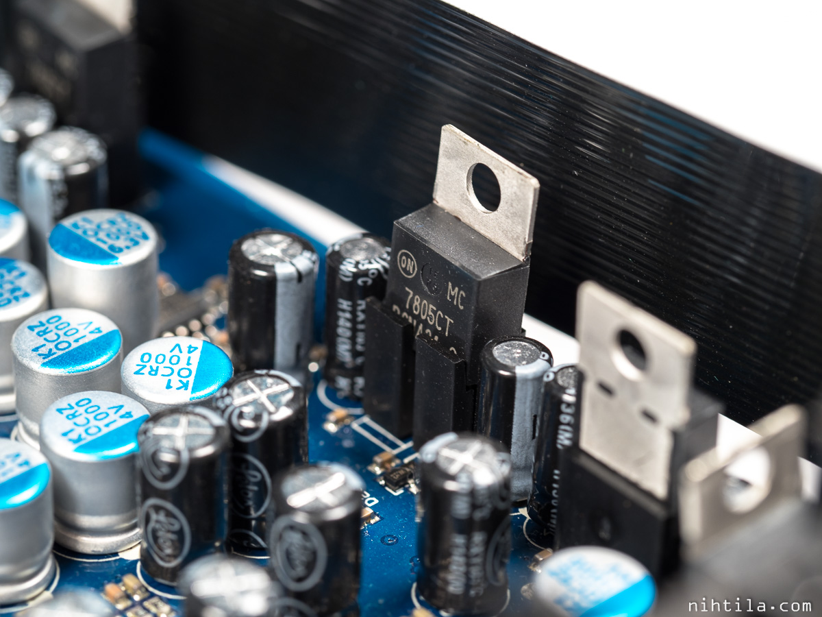
Regulators are trusty 78/79 and 317/337 series

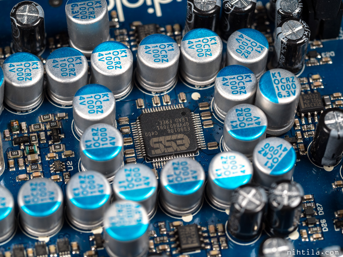
All these SMD caps around the ESS DAC are 1000 uF
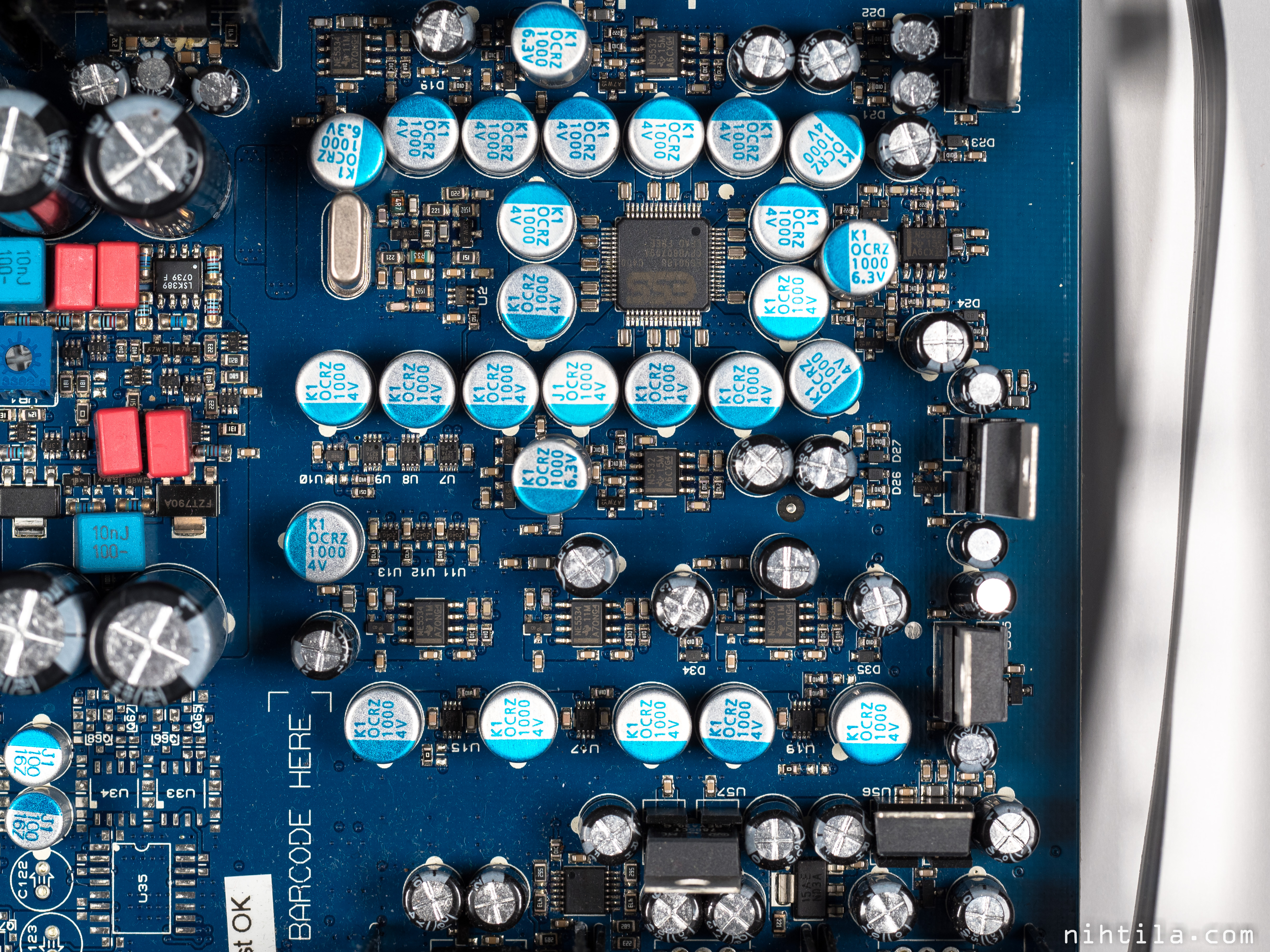
I believe pretty much all these components are related to power supplies

These are 317 and 337 regulators
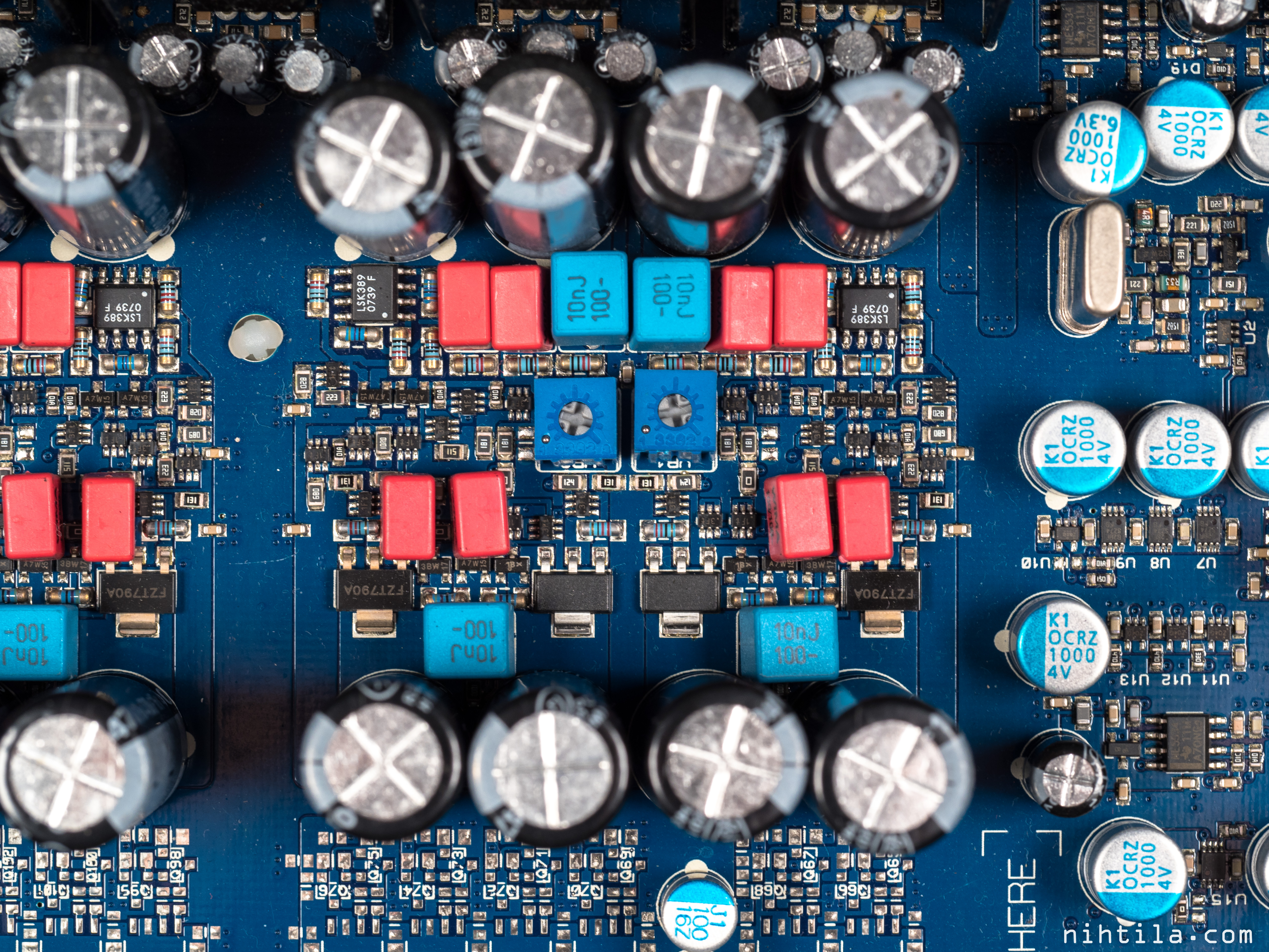
Discrete analog output stage with FETs?
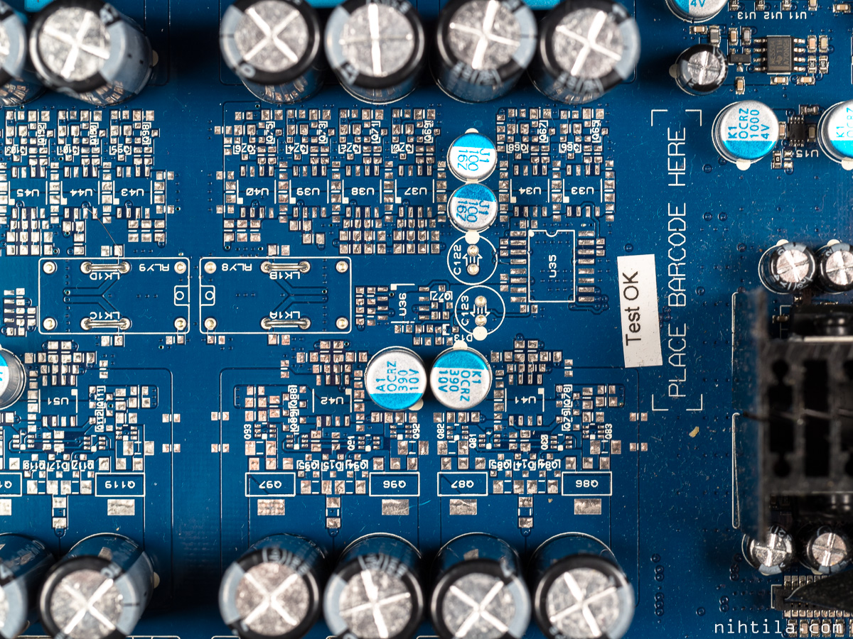
Surprisingly lot of unpopulated components

Below is the front panel PCB. There is a PIC24FJ64 but also WM8804 which is an S/PDIF transceiver. I have no idea what it is doing there. There can be some tricks going on from the USB input. Another thing with USB is that it is not only a digital input but also an interface to update the firmware.
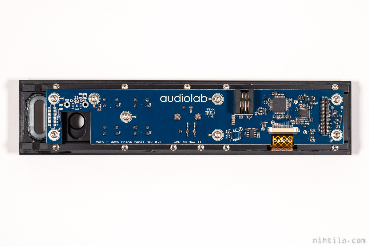
Front panel PCB

What is WM8804 doing here?
Measurements will follow later. Stay tuned!
5 comments
I’m looking forward to the measurements! Can you measure the beast with your AP?
Notification of this comment had gone to spam! But yes I will measure it with AP at some point at my work. Unfortunately I do not have my own 🙂
Those Lelon Capacitors are garbage. Exploded after 2.5 years of use. Seems that they replaced those with Nippon Chemicon.
I have M-DAC Audiolab but with broken PIC microcontroller.It is burned down.I bought new one, and I am asking is it possible to find the Hex file online, or some of you has it?
Sorry this was never answered but unfortunately I do not have the hex.
Comments are closed.