I have been using Elecrow for years as my PCB supplier for DIY projects, consisting of over two dozen designs. I have tried assembled PCBs as well so I thought of writing about my experiences with Elecrow and overall ordering PCBs from China. Recently I have started using JLCPCB as well and I will come back to that in another post at a later time.
Overall, I have been happy with the PCBs considering low prices. There has been occasional slight quality issues but these have been limited to silk screen and solder mask. I can recommend Elecrow but competition is tough though; some competitors offer even better prices and especially cheaper shipping.
This post is actually something I have mostly written at the end of 2019 but now finally publishing.
Introduction
I started doing DIY projects roughly 7 years ago. I used Iteadstudio (now Itead) for the first couple of projects but then moved to Elecrow as their 4-layer boards were significantly cheaper at the time and that’s what you really want to use in mixed signal audio. I have placed orders for around 25 different PCB designs with Elecrow. These have been from simple 2-layer power supply board to medium complexity mixed signal 4-layer board. I haven’t done any high speed digital designs so my boards are not the most demanding and don’t need fancy PCB manufacturing techniques.
I have only used KiCad for my boards which I started using in relatively early days. Therefore, I am using KiCad here as an example tool.
PCB design for manufacturing
This would be a topic of its own and I am definitely not an expert in this but here are some things to keep in mind from a hobbyist perspective when designing a PCB for manufacturing. In fact this can be split into two main goals: design for PCB manufacturing and design for PCB assembly.
Ideally, you should know the capabilities of the factory before designing a PCB. Or if the PCB is ready, choose the factory so that they can manufacture it. In practice most makers design boards that are very easy to manufacture so even the ‘least capable’ factories should be able to do them. And this is a good starting point unless you need some specific manufacturing techniques (but then you know it already).
PCB requirements
Some things to consider when designing your board:
- Layer count
- Minimum copper width
- Minimum clearance
- Minimum via size and via type (basic, microvia, buried via)
- Minimum silk screen size
- Stackup details
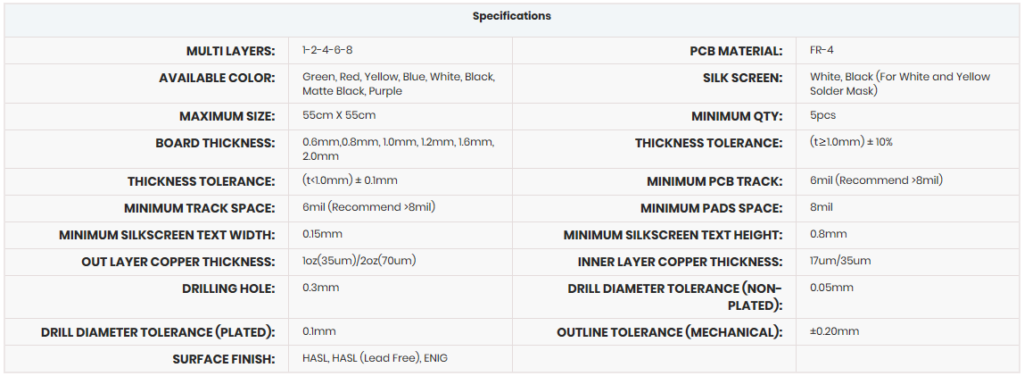
Elecrow have one of the most basic capabilities for a PCB process and if you follow those I’d say almost any factory can make the boards.
My settings in KiCad are as follow:
- Minimum trace width: 0.25mm by default, but 0.2mm on some boards where needed (8mil is approximately 0.2mm)
- Minimum clearance the same, normally 0.25mm but 0.2mm when needed
- Minimum silk screen text: 1mm with 0.15mm width for normal text
- Minimum via: 0.8mm with 0.3mm drill. This is probably the biggest drawback in Elecrow specs; this is quite large via. But minimum drill hole is 0.3mm with 0.1mm tolerance, and considering minimum track width etc. I don’t really want to go smaller than 0.8mm.
Another topic is details of the stackup for high-speed multilayer boards where impedance need to be matched. But if you’re going down that road, you know what to pay attention to. And in fact that may be a weak point of cheap Chinese PCB houses. Extra considerations are needed also for high-power PCBs where thermal characteristics become important.
Component type and placement
This is more related to PCBA but you do need to decide when designing a PCB:
- SMD components on one side or both sides
- SMD package types, especially BGAs (Ball Grid Array)
If you want components on both sides, check your factory can do this and factor in the extra cost.
Most makers use large packages for their components but some are only available in tiny BGA-type packages. Check that your factory can deal with your smallest packages. Having BGAs may also cost more. Related to tiny packages are also fancier PCB technologies with microvias, buried vias and so on. Overall you want to keep the PCB as simple as possible but sometimes there is just no choice.
There may be some limitations also how closely to one another components can be placed, especially if there are physically larger components. Check with the assembly house if in doubt.
Through-hole components may be soldered by hand so that may be priced differently. It is different process to SMD anyway.
PCB choices
There are several things you can choose when ordering a PCB, some related to the design and some just aesthetics.
PCB colour
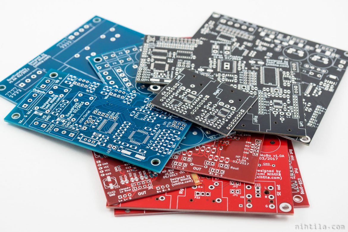
Solder masks come in numerous flavours these days, while back in old days all PCBs were green. Besides green you can usually choose red, yellow, black(ish), blue, or white. One new colour is purple and it’s often more expensive.
Silkscreen colour is usually chosen based on the solder mask colour. It’s usually white or black.
Board thickness
Board thickness is in fact not independent from the design for more complex designs. For high speed designs and impedance matching you need to know the dielectric thickness between layers.
Even if you don’t require certain thickness, thin dielectric is often beneficial. Not always though – increased capacitance can rise problems as well. However, in a 2-layer board it means ground plane and therefore return currents are closer to top layer signals. Likewise, in a 4-layer board using typical signal-gnd-power-signal stackup, increased capacitance between ground and power plane is beneficial. That being said, to really get positive effect of distributed plane capacitance the dielectric must be very thin.
If electrical characteristics requirements are not strict, it pretty much comes down to mechanical stability. Standard thickness is 1.6mm which is quite solid even in larger boards. I have used 0.8mm or 1.0mm thickness for smaller 50mm x 50mm or so 2-layer boards to get ground plane closer. However, this thin board is not very stable in 100mm x 100mm size anymore. Four or more layers make a board more solid due to added inner layers.
Copper thickness
Standard copper thickness is 1oz/35μm but can be often doubled to 2oz/70μm but the price premium may be significant. Usually the lower impedance achieved by more copper is beneficial but one should aim to do it by increasing area. Only in demanding high-current or other special applications should it be necessary to increase copper thickness.
Preparation for PCB assembly
My PCBA order last summer was my first one so there were quite some things to learn about.
A word about Chinese assembly houses
There are tons of PCB factories and assembly houses in China. Even I get quite some emails from different companies promoting their services. Sometimes it can be difficult to even know who are using the same factories as some service providers just buy the services.
So how do you rank different providers? Good question, I’d say by experience mostly. Or through the grapevine. I chose Elecrow as I had used them before. The service and quality hasn’t always been superb but I’ve always got functional PCBs in reasonably time for a very good price. Quality issues have been in silk screen and solder mask that have no impact on quality.
Package sizes
While I go for SMDs on everything, I’d say my packages are ‘medium’ size and easy to work for most factories. If they have issues with my 0603, SOT, SO, and TSSOP packages, then we shouldn’t use them at all. The good thing with these packages is also that quality is easy to check. But if you have BGAs with balls under the package, you need much better processes and on top of that you cannot visually check the end results. Although that being said, BGAs are pretty standard these days as well so you should only need to worry about smaller pitch packages. Be wary that smaller packages may cost extra.
Component sourcing
This is a topic that always arises when you google about Chinese assembly houses. As a background, when you order a PCB assembly (PCBA), there are usually two options for providing the parts: buy the parts yourself and ship them to the assembly house, or let them source the parts. When you send a BOM (Bill of Materials), you can/should state if a part needs to be original or not. For example, you want your ICs and important passives to be the exact parts you specify but generic 100nF/1uF capacitors or 1k/10k resistors can be almost anything. So all should be very clear.
Unfortunately, China is known for copying everything, whether it is a simple resistor or an aeroplane. Therefore, if the package says your specified component number, unfortunately it does not mean it really is a genuine part. The problem is that they are really good at copying things – you may not notice it immediately. Furthermore, it can be extremely difficult to prove that a part is not original; you would probably need an X-ray of an original part and the suspected copy.
Ok, so you think that the safest option is to buy the parts yourself and send them? Not necessarily. Stories tell that they may just sell those parts and use their cheap copies.
This may be a bit of a horror story but these things really happen when you investigate a bit. I think we makers need to report our experiences online, whether it is good or bad, to stop all that.
All that being said, I am not saying Elecrow would do that. But we need to be cautious.
Design for PCBA
Again I am not an expert in this (yet) as it’s my first time going through the process. However, there are some things to keep in mind when designing a PCB for factory assembly instead of hand soldering.
BOM optimisation
Not related to actual PCB or PCBA manufacturing capabilities is BOM optimisation. Although this is a different exercise for high-volume manufacturing, it’s good to pay a little bit of attention even in small batches.
For example, look at all the generic resistors (1k, 10k, 100k, pull-ups) and capacitors (100n, 1u, 10u, decoupling); some of them may be combined. For example, sometimes it may not matter if your resistor is 10k or 100k, or if your capacitor is 100nF or 1uF, and you may be able to get rid of one altogether by using the other. Also, if you need for example 5k resistor but have 10k already in your BOM, it may be better to use two 10k in parallel and so on. The same can be done for packaging if you have the same-valued components used in different packages.
For manufacturing you want to use as few unique parts as possible. Every new line in BOM costs something, while using more of a resistor or capacitor you have there already may not cost anything in practice. This is especially true for resistors; larger capacitors tend to cost more.
One more aspect is then multi-buy discount in part sourcing (if you buy them yourself). Sometimes it’s cheaper to buy 1000 resistors even if you only need 200 of them. This is another reason why using more of existing part may not cost anything in practice.
Files and information required for PCB and PCBA
To get your boards manufactured, you send the gerber files to the factory.
Gerbers for PCB
Gerber files are the manufacturing files for PCB, and you need:
- Edge cuts – PCB outline (or may be embedded in other layers)
- Copper for all layers.
- Solder mask for top/bottom layers.
- Silk screen for top/bottom, or at least top if bottom is not used. Silk screen is not mandatory but I highly recommend having clear informative silk screen. It’s one of the best things in factory-made PCBs.
- Drill files, usually two files or one combined for plated and non-plated holes.
If you do PCBA, you also need solder paste layers which are used for making stencils; or if you have a DIY reflow oven you want to order stencils as well. If you have components on both sides, you may also need adhesive layer.
It doesn’t hurt just throwing them all files you get from KiCad or other tool, they will only use the ones they need.
Files and information for PCBA
I will follow the Elecrow example here but I presume the requirements are pretty much the same with all assembly houses. Obviously, if they list some special requirements, you should respect them. Overall, give them as much information as you can and provide all files they want and wish as it will all make it less likely that something goes wrong.
Below is a capture from Elecrow website regarding their pricing and requirements.
How to charge
PCBA Quotation = PCB Cost + Stencil Cost + Components Cost + Assembly Cost + Flashing/Testing Cost.
1. PCB Cost: The price is according to the PCB layer, dimension, quantity, pads finish and your other requirements, you can check the price here.
2. Stencil Cost: The stencil is used for the soldering of SMD components. The price can be checked here, we will use the best stencil type for you accroding to the project. Please also note Elecrow will keep the stenil for three months and it won't be shipped with the assembled boards without extra requirement.
3. Component Cost: This cost is for the components provided by Elecrow. The quotation sheet given by the project manager will include exact quote for each kind of part, and it's up to you which parts to be provided by us and which parts not.
4. Assembly Cost: The price is affected by many factors such as the number of SMT pads, the number of THT pads, and the quantity of the boards. You can get the estimated price from the "PCBA Online Estimate Quote system".
5. Flashing/Testing Cost: According to the consumption of time, testing jig, and the necessary equipment for the project.
We will send you a detailed quotation sheet with above costs after receiving your RFQ and necessary files. Please note that the price calculated from "PCBA Online Estimate Quote system" is for reference only, the final price depends on the quotation sheet sent by the project manager.
What information you need to offer
Please send the following information to service@elecrow.com:
1. PCB Gerber files.
2. BOM of your project.
3. Quantity and PCB specification.
4. Parts mapping for soldering with parts machine, or a simple mapping for hand soldering.
5. Coordinate file for machine pick up parts.
6. Your specific requirements, or some tips you want to share with us to avoid mistakes.
7. Testing Plan.
8. Your shipping address and shipping method you want, DHL/FedEx/OCS/registered air mail supported.
You can download >> The template for necessary files
BOM template is given. The most important thing they want is MPN (Manufacturer Part Number) which uniquely identifies parts. They also say that you get a $20 discount on PCBA if using the BOM template but I never got this, or at least it was not indicated anywhere, and I realised it too late.
There is also another template which is actually not completely consistent with the BOM template. This one contains everything in one multi-tab spreadsheet: BOM, part identification, POS file, and shipping details.
BOM
Bill of Materials lists all your components required for assembly. It should have following information:
- Reference designator
- Manufacturer part number (MPN)
- Package
- Description
- Original yes/no to indicate if part is swappable
- Order code, preferably two sources such as Mouser and Digikey
Original column states whether your part must be exactly the given MPN or can it be swapped to something similar.
POS file
POS file tells where a component is located on the PCB; it lists your component coordinates and orientations. Reference designators must match BOM. This is automatically generated from a CAD software like gerber files.
Contact and shipping details
Shipping address to ship the PCBA box and email address to send the quote to.
Elecrow experience
As said, I’ve ordered a lot of PCBs from Elecrow, from 20mm x 30mm 2-layer boards to 100mm x 150mm 4-layer boards. Relatively simple, no BGAs or extremely small components. I have used the same above-mentioned design rules for all boards.
PCB quality
First of all, all boards have worked. Electrically I have not faced a single issue on my boards.
Quality has not been consistent but all boards have been functional. Quality issues have been mostly on silk screen or something small on solder mask and hole tolerance. All within specification probably as it’s quite loose. Therefore, considering the price all this is a bit of nitpicking.
Overall 4-layer boards have been of better quality. The process is different due to extra layers but it seems also silkscreen and solder mask are done differently.
Silkscreen
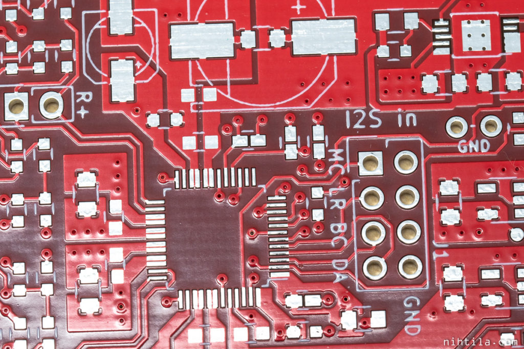
Below are some examples of PCBs. One of the worst ones I got when they had a discount offer of 10pcs 100mm x 100mm 2-layer board for $4.90 or something ridiculous (which seems to be more standard even now).
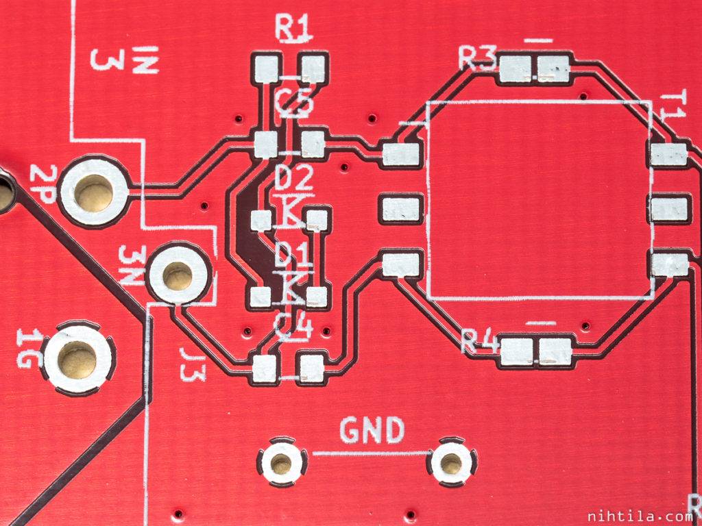
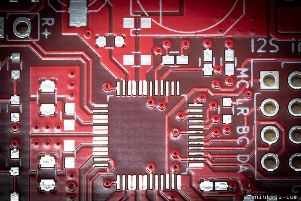
Below it can be seen that silkscreen print on 4-layer board looks different. It’s smooth, while on 2-layer board above you can see pixels in the letters.
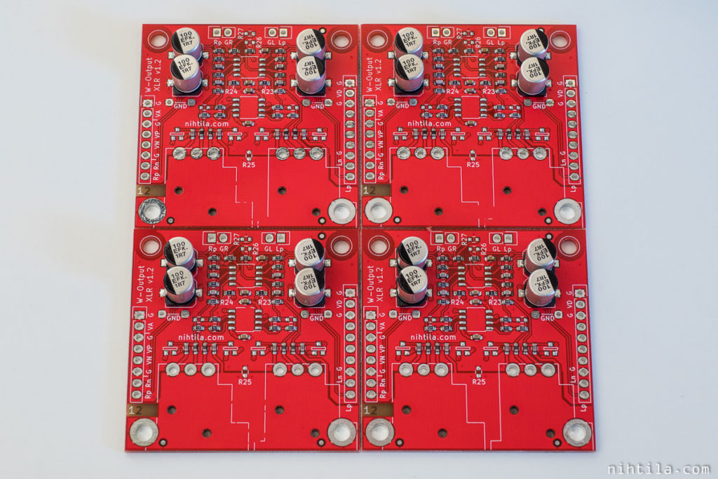
This design which was part of PCBA also showed odd silk screen inconsistencies. Look at the XLR outlines on bottom edge of the boards; only the bottom right PCB have solid outlines but all other three have cuts in the lines. This is actually even a 4-layer board.
Solder mask
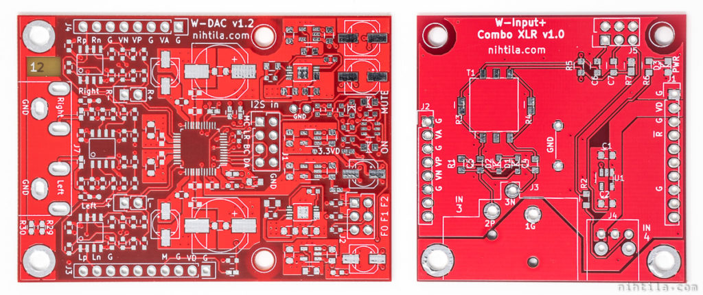
Solder mask colour is also not completely consistent, their red is different red in 2-layer and 4-layer board; one is more orange. Again, this may be related to the process I don’t know about.
I have also ordered ‘black’ PCBs from Elecrow and these are not actually black but dark brown and do not look very nice but more like dirty. Also the solder mask wasn’t completely even which made it look even more dirty. I wouldn’t recommend that. I have not tried the matte black option though.
Elecrow have been asking for minimum solder mask clearance of 0.2mm which is huge in today’s PCBs. It means that many ICs don’t have solder mask between pins at all. It can be seen below on one of my older 2-layer boards.
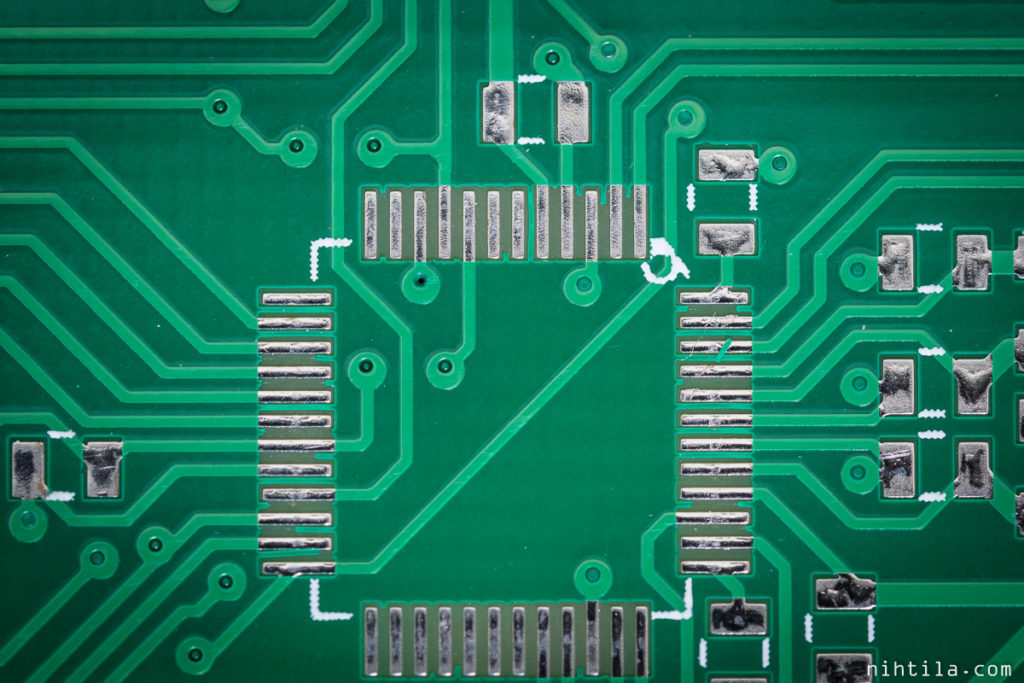
However, below is one of the newer 4-layer designs. There is solder mask between pads. I have been using 0.2mm clearance in KiCad as that’s what they have been asking – so there is no solder mask between pins in my Gerber files. It seems they have adjusted the solder mask on these apparently tighter-tolerance 4-layer PCBs.
These solder mask ‘issues’ don’t have a real meaning, these are just observations. I just hope they would tighten the specs if they can do it better. That being said, if the spec is loose and we follow it, our PCBs should be reliable.
Stencils
Since building my own reflow oven I have started ordering stencils for applying solder paste. Elecrow stencils are very good quality stainless steel stencils for little money. I also like that you can get small 15x15cm stencils without frames.
PCB assembly
I used Elecrow’s templates as a starting point. I made my BOM (approximately) as the template and then added the BOM, POS file, visual identification, and shipping and contact details in one multi-tab spreadsheet.
The spreadsheet is send to Elecrow using the PCBA link. You can also use the online calculator for approximated PCBA cost.
After around 12 hours I got a quotation back. It was based on the same spreadsheet I sent with clear cost breakdown: PCBs, assembly, parts, and shipping. Very clear and easy to see what things cost. If you’re happy with it, you go back to the PCBA page linked above, and just type the USD sum to the Qty of $1 ‘items’, your project manager’s name, and order. Finally reply the order number to your project manager.
After all this I got confirmation that my order is placed and manufacturing will start soon. 3-4 weeks lead time was given.
Diagram below is from Elecrow website illustrating the order process. I did not outsource any testing as the boards were not fully populated at this point. Moreover, testing high performance analog circuits is not so straightforward or requires very capable test kit (depending on the level of testing required, of course).
After two days I got a question that there is something wrong with my silkscreen and if I want to continue. It appeared they interpreted silkscreen, fab, and courtyard layers all as silkscreen which of course becomes very messy. I’m not sure what is the standard interpretation but I thought it would be clear SilkS layer is silkscreen. Anyway, good they asked before doing anything silly. This is just one example that there are actual humans checking the files as mentioned.
PCBA took a bit longer than the given 3-4 estimation.
PCB shipping and delivery time
Speaking of just PCBs, it usually takes around a week to manufacture PCBs. If using a courier for shipping, then it’s a few more days to deliver so I count around two weeks overall although it may be slightly faster. If using slower/cheaper shipping method, then it can take significantly longer.
One pain with courier is that they take their own fees for customs declaration and depending on country you may have no other option to do it. If you opt for snail mail, you may avoid customs and paying VAT, or you may need to pay VAT and need to pick up your parcel from a remote customs office location, again depending on your country. So your choice, courier is the easiest, faster, and consistent but also consistently more expensive.
And courier prices at Elecrow especially seem to be pricey. In fact, I’m quite sure they have got more expensive over time. Now if I order a few 10pcs PCB designs, I end up paying something like 70-80 dollars for shipping for a small parcel which is silly. Then come DHL and add their own fees for customs declaration.
Conclusions
Overall I have been happy with my PCBs. I wouldn’t have ordered so many times otherwise.
However, I guess you get what you pay for. Quality is not the best but good enough for us and they work. And you really don’t pay a lot. And that being said, quality of 4-layer boards have been very good.
Annoying thing always in ordering from China is that shipping fees are so high relative to the product. And couriers’ customs fees are frustrating.
I have actually written most of this stuff around 8 months ago already. But now recently, in summer 2020, I have started looking at JLCPCB and am just waiting for my second order from there. They offer amazing prices at least at the moment and their shipping fees are lower. They do have premium in some PCB color/layer count combinations or if you need tighter tolerances. I will write about them at a later time when I have a bit more experience. I am still using Elecrow as well though, for example their stencils are smaller and castellated holes cheaper if you need those.

2 comments
very good and informative review !
I didn’t go for PCBA yet, and regarding my PCBs (2- and 4-layer as well) I am still stuck to eurocircuits.com up to now,
because I do not yet dare to order in China 😉 (but I’am very interested to do in future)
you can just upload your native eagle- and kicad- files (no hassling with gerbers), it’s very fast, quality is very high, you can get very tiny vias/tracks/spacing, very reliable, but of course very expensive … 😉
Thanks, this is indeed something I wrote a long time ago but just never published. And as mentioned, there are even more competition in that space now than 8 months ago or so when I wrote that. And that means better products for better price for us.
I just got my second JLCPCB order and the boards look very good again. It does look like they have better quality for really low prices, at least for now. It’s also handy to have DDP delivery option where they take care of all duties and taxes so you pay those already when ordering; along with a fee but so does DHL take fee for customs handling.
Comments are closed.