
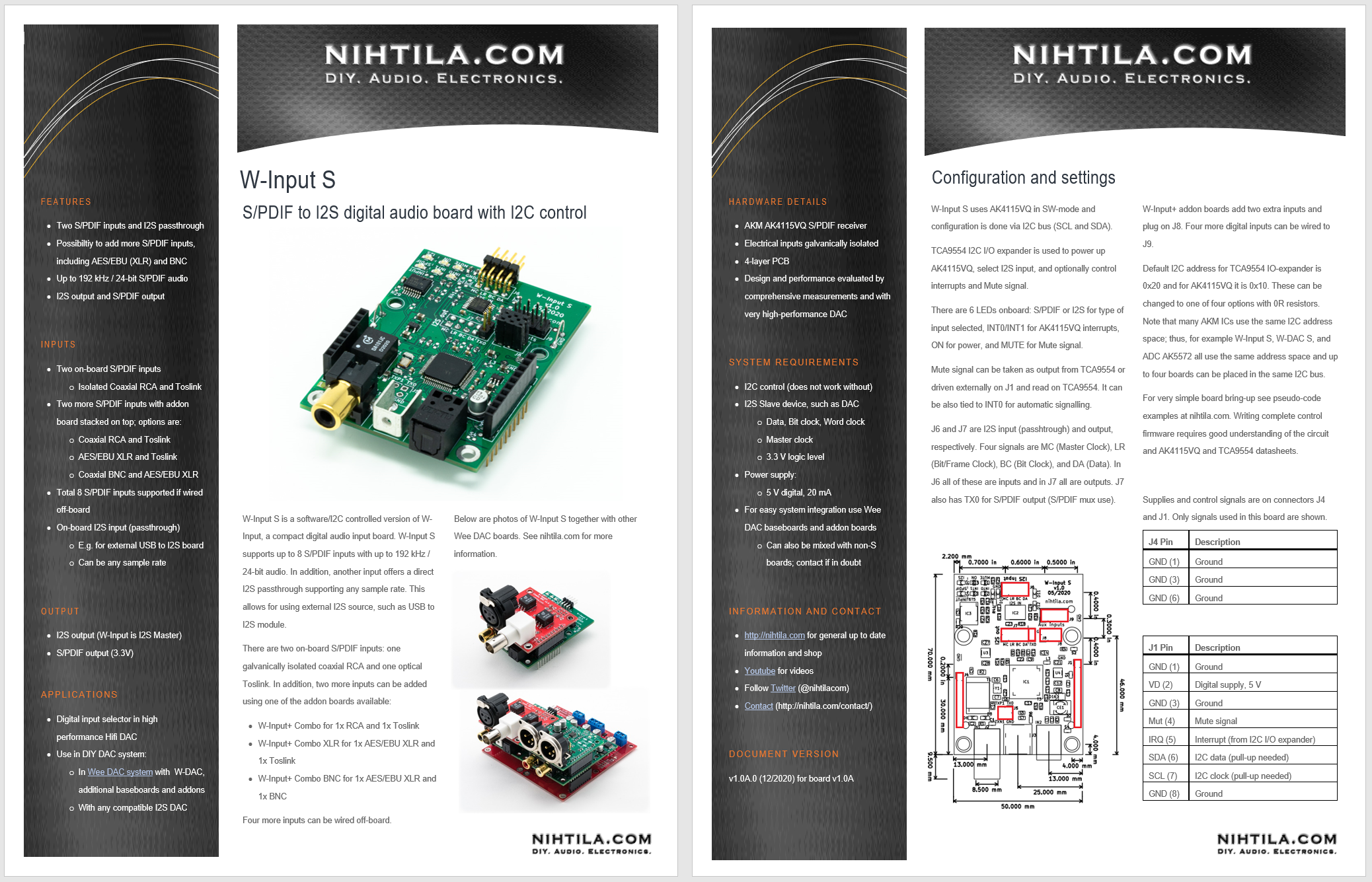
This is a software-controlled version of W-Input compact S/PDIF receiver board. It offers basically the same features but requires control and setup via I2C bus. Note that control software is not provided but is required to get any audio out.
- Flexible digital input board combines I2S input and S/PDIF inputs
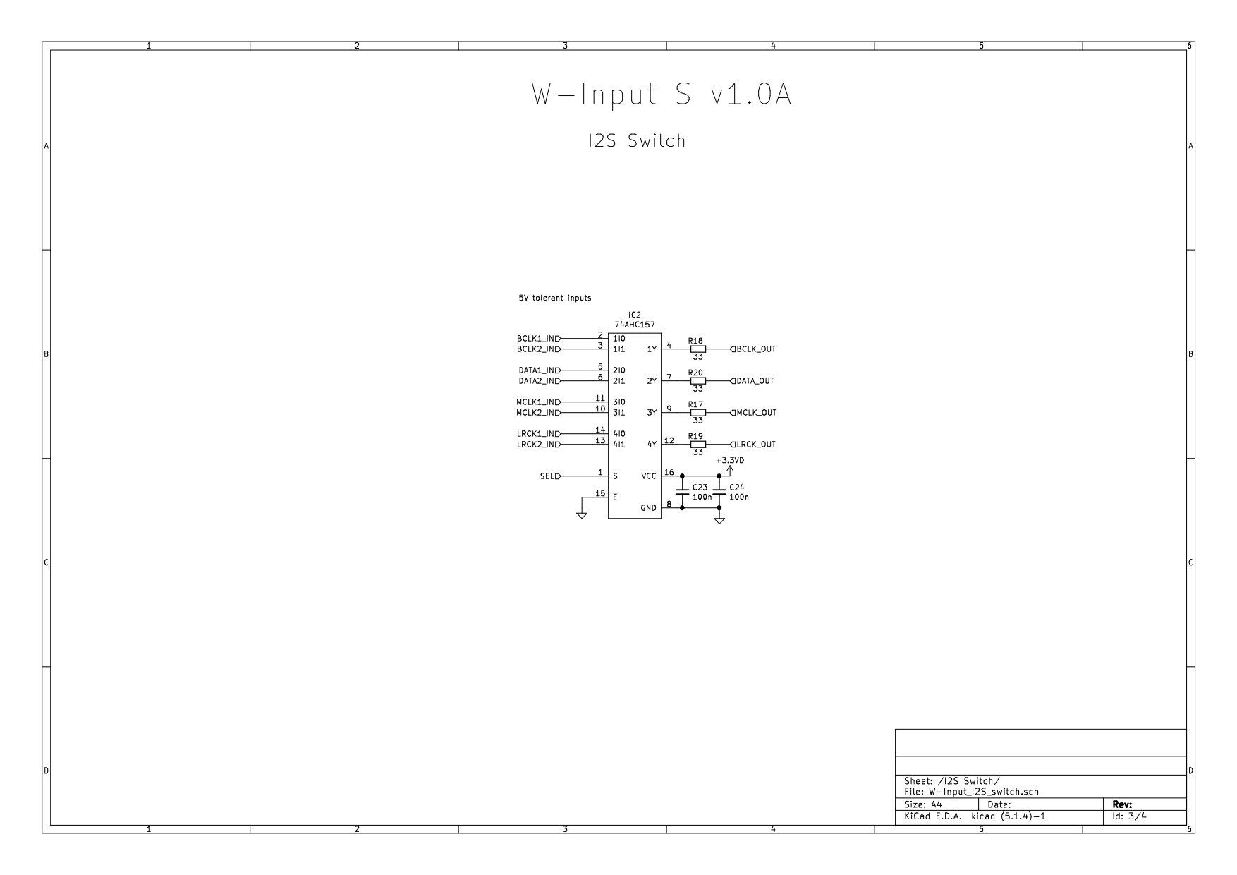
- One I2S input / passthrough
- One Toslink S/PDIF input
- One isolated coaxial S/PDIF input
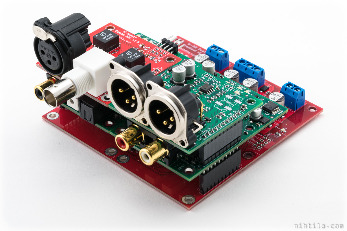
- More inputs (Toslink / Coax / AES/EBU) can be added with addon board
- I2S output (up to 192 kHz / 24-bit from S/PDIF)
- High performance to match with high performance DACs
- AK4115VQ S/PDIF receiver
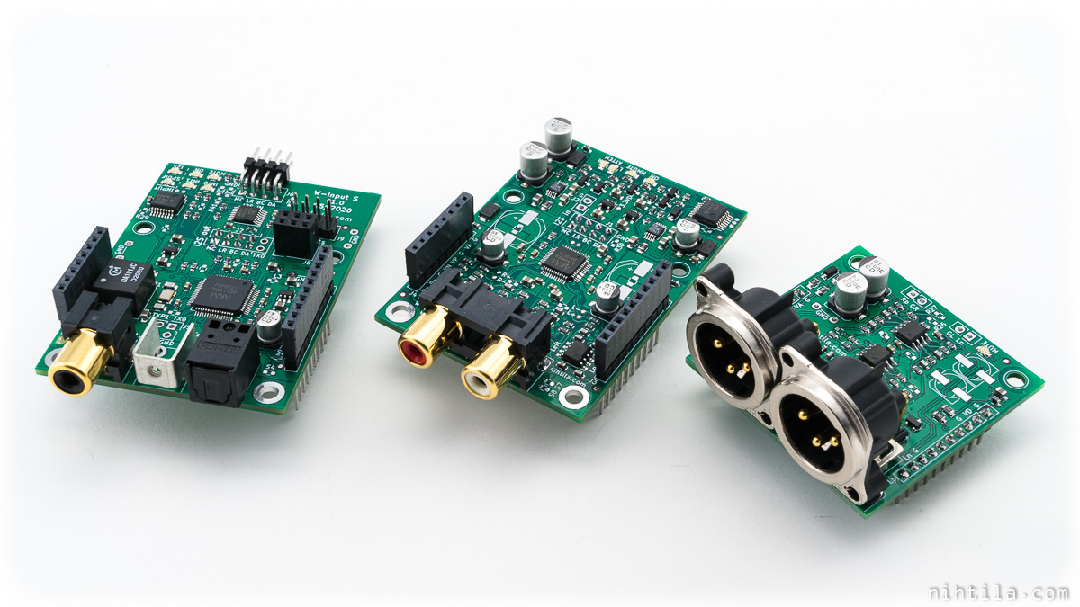
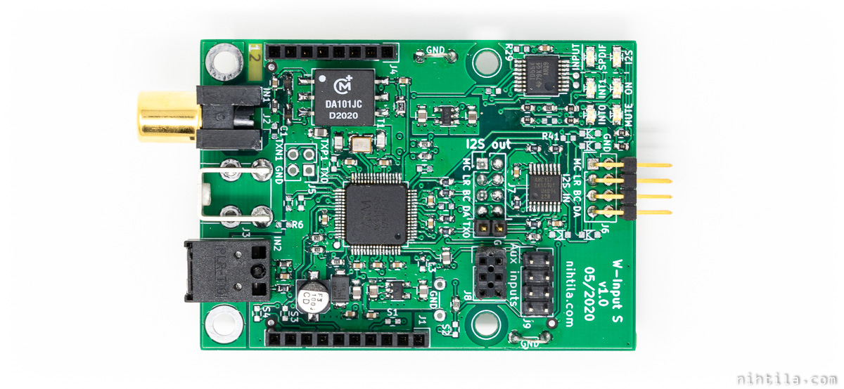
- Compact size at 70 mm x 50 mm
- Can be used with W-DAC, W-DAC S, or any compatible I2S-input DAC
- Wee DAC ecosystem offers numerous compatible boards
- Assembled boards available
W-Input was designed as part of Wee DAC ecosystem but it can be used in any system providing needed supplies and compatible I2S signals. By using other Wee DAC boards, complete DAC with extensive digital input options as well as balanced XLR outputs can be built.
Below is a 2-page factsheet (PDF) showing key figures and features.
This board is part of Wee DAC system, find more here.
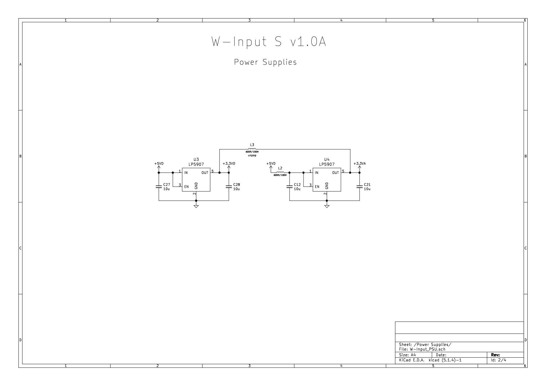
Design
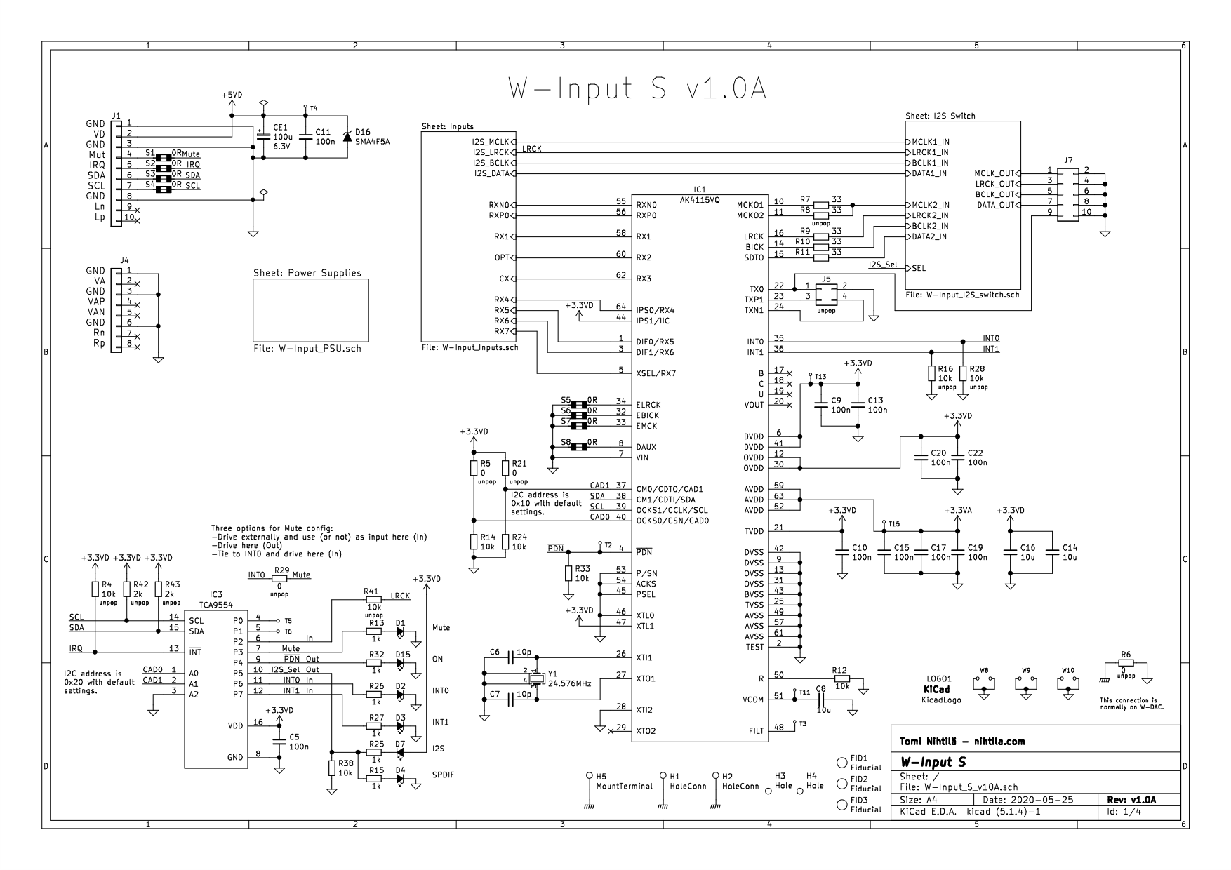
The design closely follows W-Input. The main IC is AKM AK4115VQ S/PDIF receiver with input mux and it is controlled via I2C bus. In addition, TCA9554 I/O expander is used for some additional control while maintaining backward-compatible Wee DAC interface in the 1×8 and 1×10 pinheaders.
Inputs
There are one Toslink S/PDIF input and one transformer isolated coaxial S/PDIF input onboard. In addition, there is a pinheader J8 for two extra S/PDIF inputs using one of the Input+ addon boards. Moreover, this I2C version has J9 where you can wire four more S/PDIF connectors as it is possible to use 8 inputs in I2C mode, while pin-control mode only allows 4. However, not more than one input addon boards can be stacked on W-Input S, so you would need to wire these off-board.
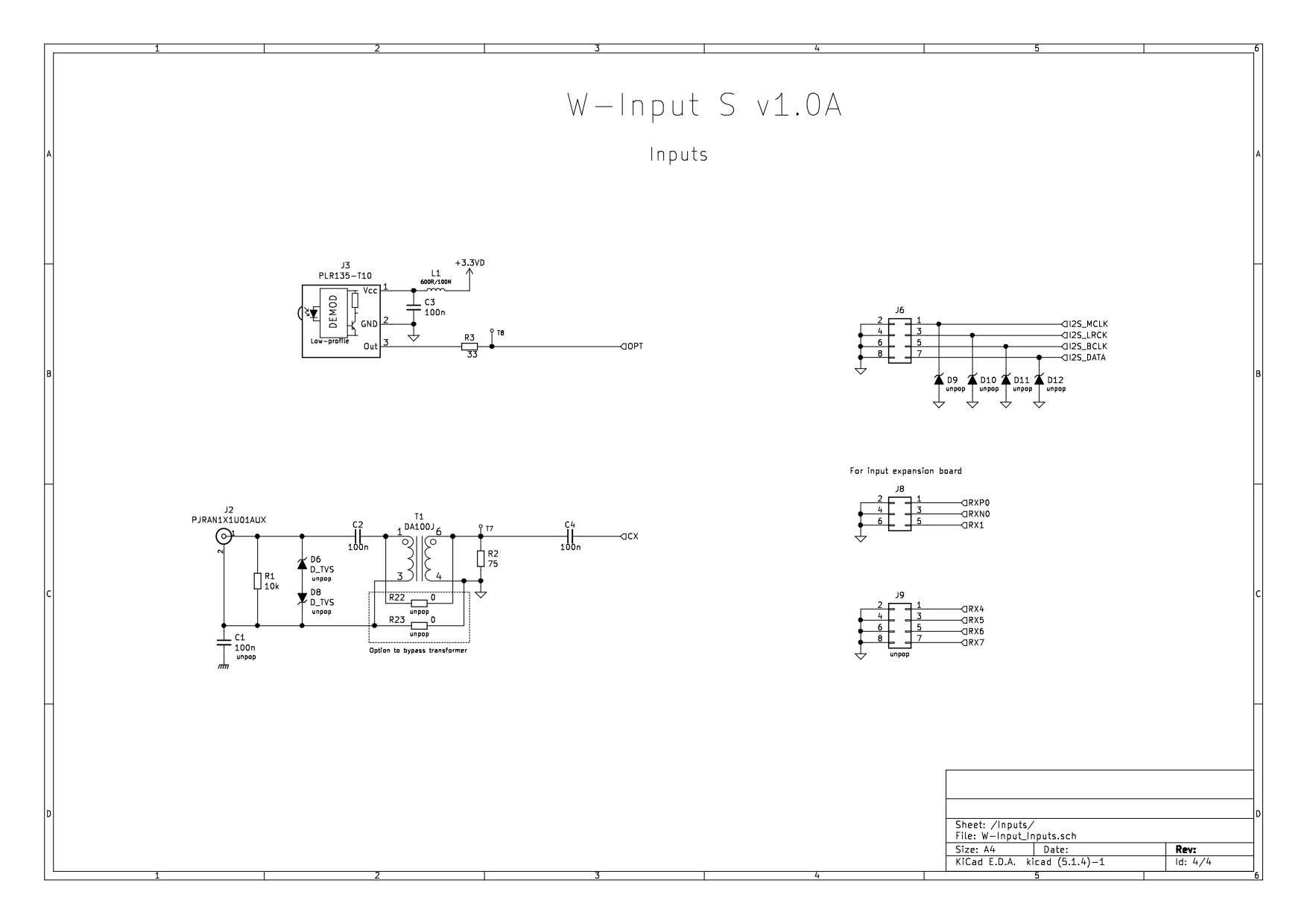
I2S input is routed directly to the I2S switch. Therefore, it basically bypasses everything on this board and goes directly to I2S output.
Control
Control is done via I2C signals SCL (clock) and SDA (data). Instructions for controlling AK4115VQ along with its register map is given in AK4115VQ datasheet. Moreover, there is also TCA9554 8-bit I2C I/O expander on-board to help control some of the other things outside the receiver chip. Default I2C addresses are shown in the schematics, and they can be changed with resistors. Four different addresses can be given to a W-Input S board.
Note that W-DAC S has the same address space so four W-DAC S or W-Input S boards can be used in the same I2C bus. Also AK5572 used in ADC AK5572 is using the same address space; presumably most AKM ICs use the same address space.
TCA9554 is used for following functions:
- Power up DAC IC (PDN pin, high means power on)
- I2S input select (low means I2S select, high S/PDIF selected)
- Mute signal (see more below)
- Read AK4115VQ interrupt pins
Note that I2C and IRQ pull-up resistors are not populated by default, assuming that they are at the host side. Ensure pull-ups are in place somewhere in the system.
Mute signal
Mute signal is a bit more complicated as the system leaves options how to use it. Mute is one of the fixed signals in the 1×10 edge pinheader along with SCL, SDA, and IRQ, and thus goes to all boards stacked together (such as W-Input and W-DAC boards). The same mute signal is also there in non-I2C versions of W-Input and W-DAC, where the source is W-Input and mute comes from INT0 – and that is also possible here by populating R29. In this case no other Mute control is needed.
Overall, you can take Mute from AK4115 INT0, or you can drive it directly from a host/outside, or you can take it from the TCA9554 by configuring it output. The choice is yours. For sort of automatic function, tie it to INT0 and unmask INT0 flags you want to trigger Mute. For full host-operated mute, take the Mute signal from a host controller.
Mute signal does not have any functional meaning in W-Input (S) but it is used in W-DAC and W-DAC S to mute the outputs. If you don’t use W-DAC or W-DAC S, you don’t necessarily need to care about the Mute signal.
No USB input?
No, unfortunately still no USB input. Creating a high-resolution USB input is not a simple drop-in IC task, and I don’t have a solution yet. I would want to investigate that option later but for now the solution was to add I2S input for an external USB to I2S module.
PCB
Form factor is the same as W-Input and PCB is a 70 x 50 mm 4-layer board.

As usually, schematics and layout have been done with KiCad. PCBs are from JLCPCB. Colour changed to green as JLC had so good discounts which didn’t apply to red boards. It’s also good to easily distinguish from non-I2C counterparts. Components are sourced from Mouser and Digikey.
I2C control
I do not provide control software. If you buy a board, you need to take care of this yourself. However, if you have ever done anything similar, it is a rather straightforward task. Here are some tips to get started.
Your best friend here is AK4115VQ datasheet and TCA9554 datasheet to see how to set up the DAC and I/O expander, respectively. But in order to get started, I have listed here a few lines of writes that get you up and running.
First of all, note the I2C addresses. These are defaults and can be changed with resistors R5, R14, R21, and R24; the resistors control the two least significant address bits of both ICs.
- AK4493: 0x10
- TCA9554: 0x20
Also remember that I2C bus needs pull-up resistors. If your host side doesn’t have them, populate R42 and R43.
I have used here syntax Write(I2C address, register address, data). In fact, I use Analog Discovery 2 when testing devices with I2C and that’s how it is written there as well.
TCA9554 setup
Below is a simple setup for TCA9554.
// Following lines power up AK4115 and set S/PDIF input.
// All pins are input at startup.
Write(0x20, 0x03, 0xCF); // set I2S_SEL and PDN outputs, the rest inputs
Write(0x20, 0x01, 0x30); // set both outputs high to enable S/PDIF input and power-up AK4115
In this example Mute is not controlled by TCA9554 but come outside from host. You can also control mute with TCA9554 by setting this pin output.
TCA9554 also has IRQ for input pins. This can be used with input pins connected to INT0 and INT1; see TCA9554 datasheet for more information.
AK4115VQ setup
// Set up receiver with similar settings to W-Input
Write(0x10, 0x00, 0x0B); // Set clock and MCLK settings
Write(0x10, 0x01, 0x5A); // Set up interface

// I2S input select, 0x50 = RX0, 0x51 = RX1 and so on; RX3 = RCA
Write(0x10, 0x03, 0x53); // Select onboard RCA input (RX3)
Update 10/10/2022: There was an error setting register 0x00 to 0x0F and register 0x01 to 0x5A. It kept MCLK always at 128xFs, leading to too low MCLK at lower sample rates. This worked (at least with AK4493) but caused performance degradation at lower sample rates. This can be fixed by changing OCKS bits in register 0x00 or ACKS bit in register 0x01. This should keep MCLK at 24.576MHz for all 48k/96k/192k sample rates.
That’s really all you need to get I2S audio out from RCA S/PDIF input. You can also read sample rate information, configure TX S/PDIF bypass output (to use W-Input S just as S/PDIF mux), read additional metadata bits, configure INT0 and INT1 interrupts, etc.
Measurements
Several measurements have been carried out on this board but there is not much relevant info to show. After all, the best praise for this board is that it has no impact on system performance. And this is the case even with a very high performance DACs.
However, to ensure correct operation following tests have been carried out:
- Functional tests with 44.1 kHz, 48 kHz, 96 kHz, and 192 kHz sample rates
- Signal integrity measurements on S/PDIF and I2S signals; also ensuring S/PDIF transformer does not compromise signal quality
- Functional tests of reset and mute circuits
- Functional test of all inputs, including W-Input+ addons
Impact on audio performance
I have not seen this board being a bottleneck of a complete DAC system, and that is perhaps the best measurements result possible for a board like this. I have measured a DAC up to -115 dB THD+N and -115 dBV RMS noise floor, comparing DAC I2S input and W-Input, and noticed no difference between the two.
Power consumption
W-Input S takes around 25 mA from 5 V supply VD. If using TX (S/PDIF) output and driving terminated coaxial line, current consumption increases significantly.
Files
References and additional information
- 2-page factsheet
- AK4115VQ datasheet
- TCA9554 datasheet
- W-DAC S
- W-Input (older non-I2C version)
- Wee DAC system
Version history
Schematics / PCB version history and known errors and bugs
- v1.0A Initial version
This page version history
- 28.12.2020 Initial version
- 10.10.2022 Correction to AK4115VQ register writes
Buy boards here.