
- Simple balanced buffer with very high performance
- Noise level: -117 dBV A-weighted (v2.0B)
- THD+N ratio at 2 Vrms output signal: -119 dB (v2.0B)
- Two versions can be populated:
- v2.0A – traditional balanced output with inverted signal on cold lead
- v2.0B – simplified output with ground on cold lead
Original Addon BalOut was designed for H-DAC but as there has been interest in those boards, this new version is easier to use in other applications:
- No filter components
- Normal opamps instead of fully differential opamp
- Separete input signal pinheaders
- Mounting holes
- Reference designators on silk screen and cheaper 2-layer board
Design
Addon BalOut v2 is a balanced buffer based on the previous version of Addon BalOut with some notable differences to make it more general purpose. Original version was designed for H-DAC and contained filter components as it was part of 3rd order low-pass filter. While this v2 can still be used with H-DAC, it is easier to use in other designs as well; some DIYers have been asking for boards for their own applications. It does not have any filter components, just buffers with gain-setting resistors.
Input is fundamentally differential, however, cold lead can be ground – it can be used as single-ended to differential converter. Input CMRR will not be extremely high, therefore it is better to be used close to signal source.
Previous version had fully differential opamp but here I have used conventional opamps. There are two options for population of this board:
- A: Dual-buffer design where cold output lead is inverted replica of the hot lead. This is how most want their differential signal to be.
- B: Single-buffer design where cold lead is effectively ground. However, due to identical outputs resistors on both leads, this design is effectively balanced as well.
Balanced interconnects are often slightly misunderstood why most want cold lead to be actively driven with the inverted signal although it is not necessary for benefits of balanced interconnection. The key idea is impedance balance which does not require the inverted signal. I use balanced interconnects in all of my designs and have moved to use designs similar to the B-version as it is simpler and cheaper to make.
Gain can be adjusted as per conventional opamp circuits. If populating A-version with inverting opamp, ensure both opamps have identical gain. The examples shown use 1 kΩ resistors everywhere. Therefore, A-version has 6 dB gain and B-version 0 dB.
Output consists of clamping diodes for protection and RF-filter. These are optional and can be left out.
Dual opamp A-version
Uses two opamps from which one is inverting the signal to drive the cold output lead. This also gives 6 dB higher signal level if resistors are otherwise the same.
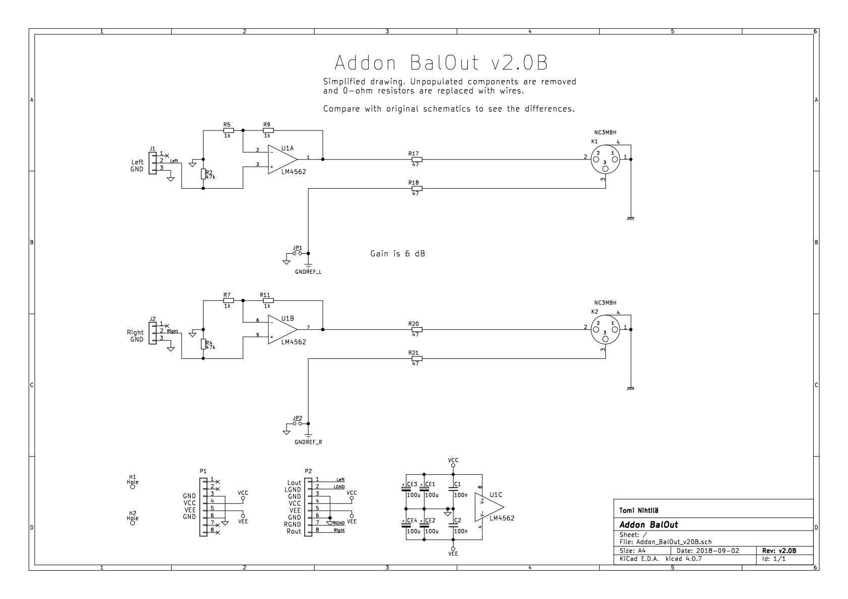
Schematics
R18 and R21 are unpopulated, otherwise all components on board are populated. Basically any opamp will work but LM4562 is one of the best-measuring opamps and still reasonably priced. For the ultimate bang-for-buck opamp, choose NE5532.
Pinheaders P1 and P2 are to support H-DAC but are also used for supply connections. When not used in H-DAC, J1 and J2 can be used for input signals. If using single-ended connection, connect signal between Left/Right and GND pins. If using differential signal, also shield can be connected.
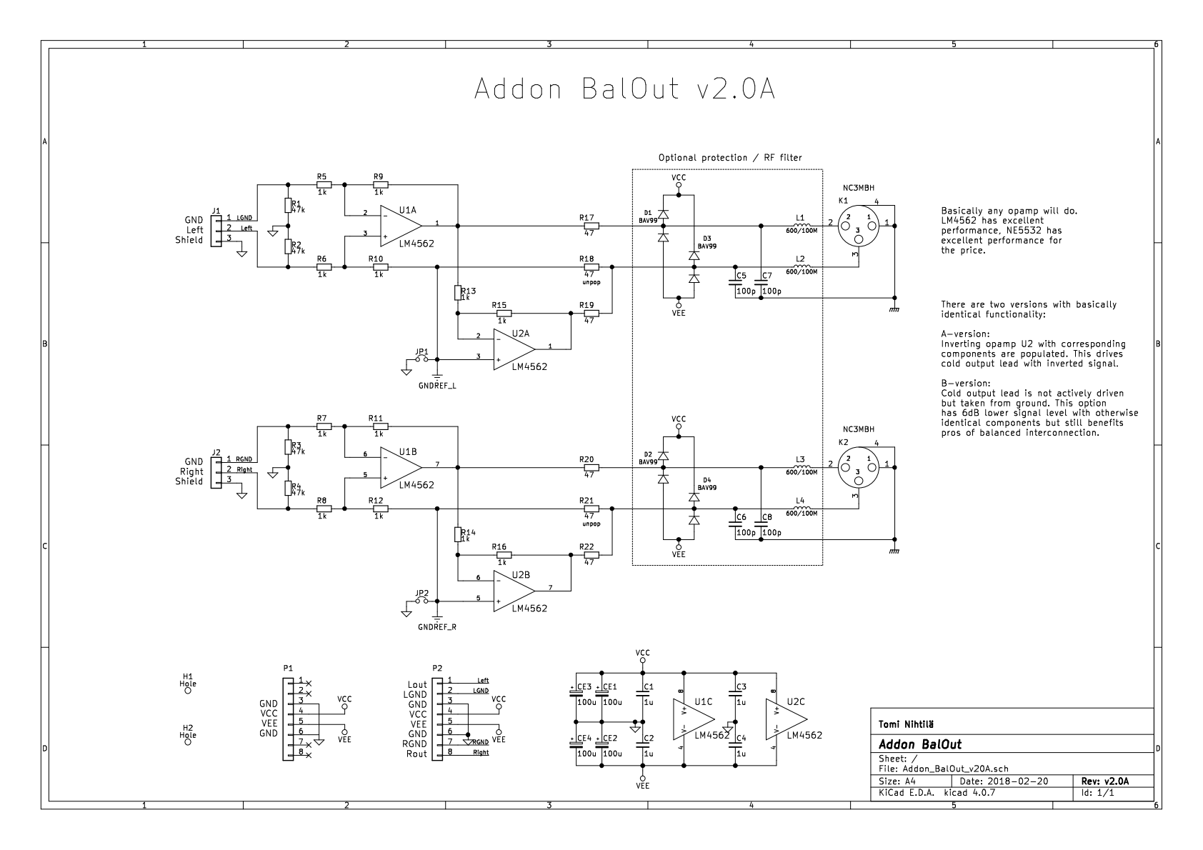
v2.0A schematics
Population
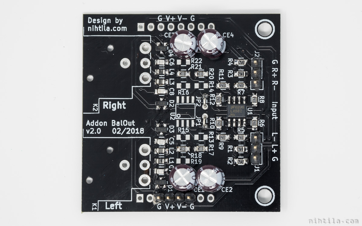
Below is a fully populated A-version board used in the measurements. As can be seen, only part of P1 is populated for supply connection (bottom edge of the board on photo).
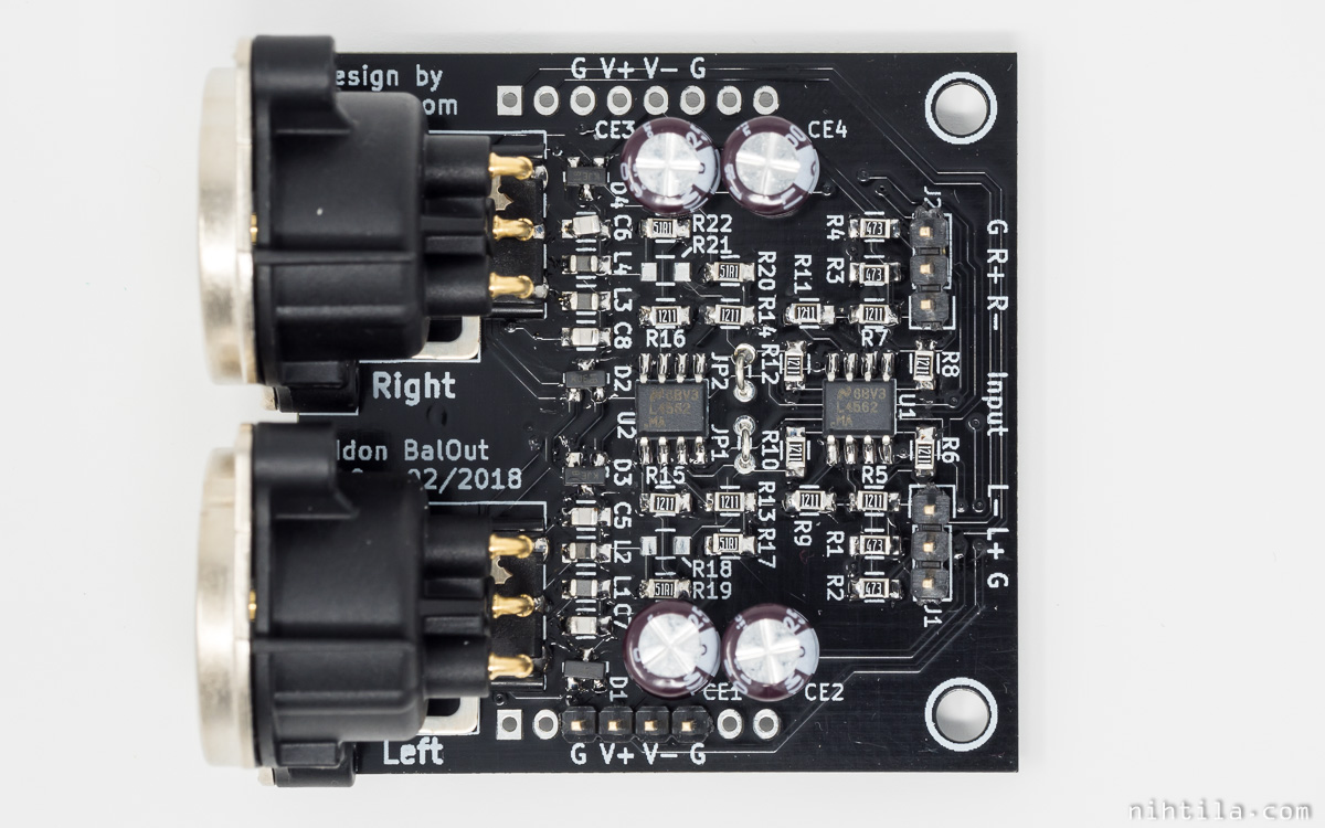
A-version populated
Edit 5.9.2018. For very simple single-ended to balanced conversion, simplified population as shown in the schematics below can be used.
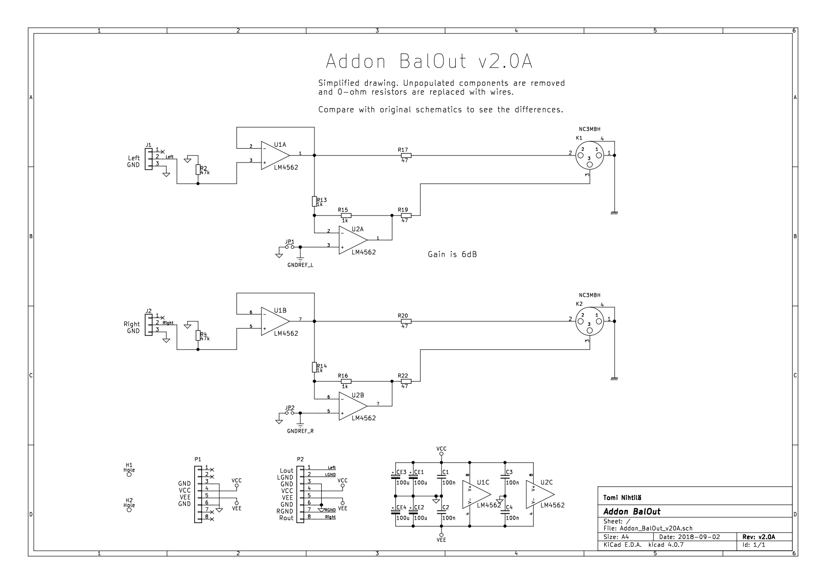
V2.0A simplified schematics for single-ended to balanced conversion with 6 dB gain
Single opamp B-version
This version uses only one opamp per board. Cold lead is taken from the ground reference via output resistor. Gain with shown resistor values is 0 dB.
Schematics
Here R18 and R21 are populated but U2 and its external components are unpopulated.
As in A-version, any opamp will work but LM4562 is one of the best-measuring opamps and still reasonably priced. For the ultimate bang-for-buck opamp, choose NE5532.
Pinheaders P1 and P2 are to support H-DAC but are also used for supply connections. When not used in H-DAC, J1 and J2 can be used for input signals. If using single-ended connection, connect signal between Left/Right and GND pins. If using differential signal, also shield can be connected.
If you want to take single-ended output, use this B-configuration and replace R18 and R21 with 0-ohm resistors or shorts.
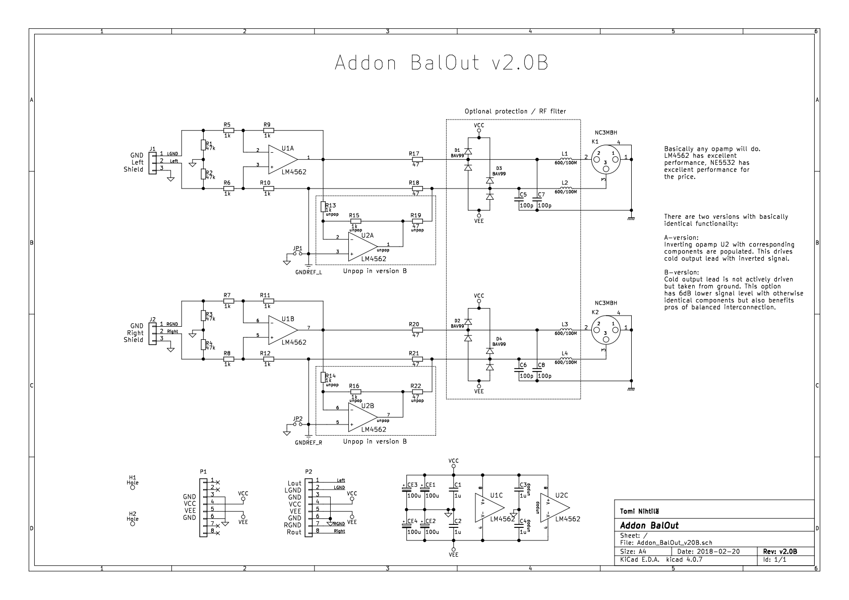
v2.0B schematics
Population
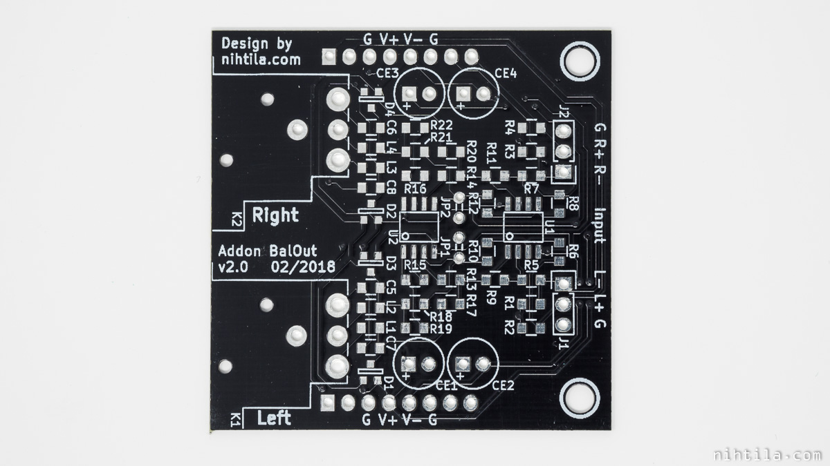
Below is a B-version board used in the measurements, without XLR-connectors.
B-version populated without XLR-connectors
Edit 5.9.2018. For very simple single-ended to balanced conversion, simplified population as shown in the schematics below can be used.
V2.0B simplified schematics for single-ended to balanced conversion with 6 dB gain
Layout
PCB is 2-layer 50×50 mm and 0.8 mm thick. It contains pinheaders to still support H-DAC but also separate input pinheaders and mounting holes as opposed to the version 1.
As usually, schematics and layout have been done with KiCad and PCBs ordered from Elecrow. Components are sourced from Mouser.

Layout with ground plane hidden
PCB top
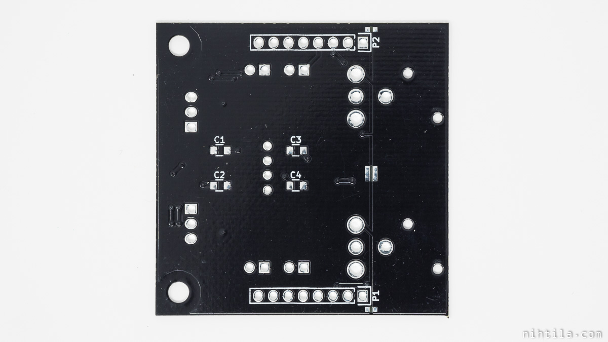
PCB bottom
Measurements
I have measured the board at work using Audio Precision APx555 audio analyser. Unless otherwise mentioned, measurement bandwidth is 20 kHz and frequency in single-tone measurements is 1 kHz. The board is powered by a bench PSU.
These results are taken with differential input but I also ran the measurements with single-ended input and differences were minimal.
v2.0A vs. v2.0B
A-version has inverted opamp populated, while B-version does not. Otherwise same component values have been used, therefore A-version has 6 dB more gain and corresponding effects seen on measurements.
Key figures
Measurement conditions
- A-weighted noise level (20 kHz bandwidth):
- A-version: -109 dBV (6 dB gain)
- B-version: -115 dBV (0 dB gain)
- THD+N ratio at 2 Vrms output level (1 kHz signal, 20 kHz BW):
- A-version: -115 dB
- B-version: -119 dB
- Crosstalk: -128 dB at 10 kHz
- Current consumption (±14 V supply):
- A-version: 21 mA per supply
- B-version: 11 mA per supply
Noise level is given instead of SNR as latter depends on the signal level.
THD+N
A-version
With inverted opamp, 6 dB gain.

A-version THD+N level vs. output level
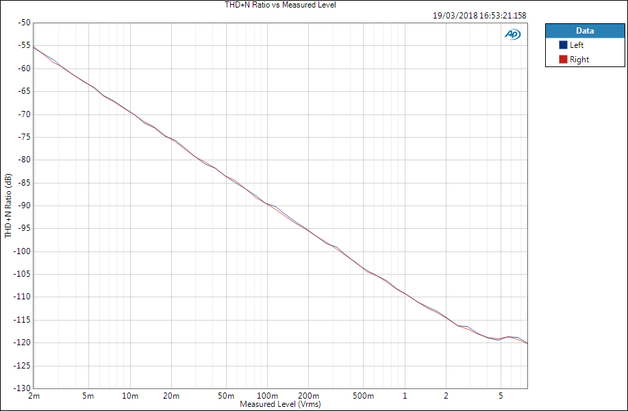
A-version THD+N ratio vs. output level
B-version
Without inverting opamp, 0 dB gain.
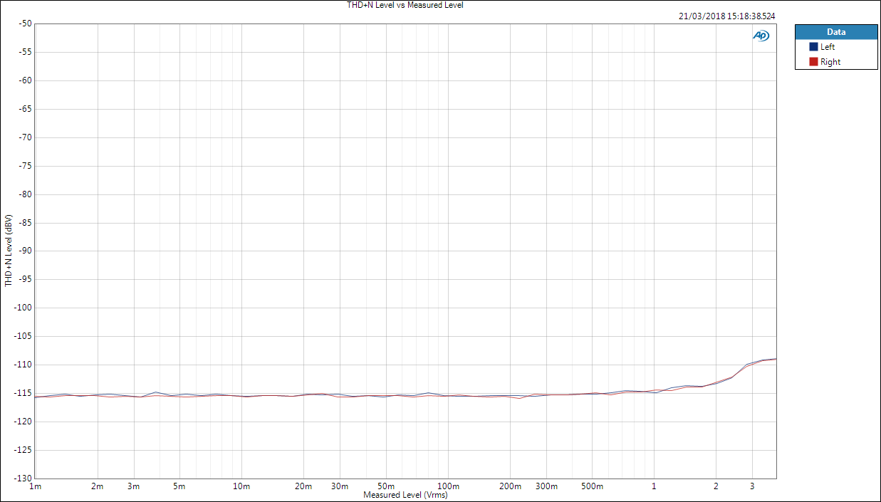
B-version THD+N level vs. output level
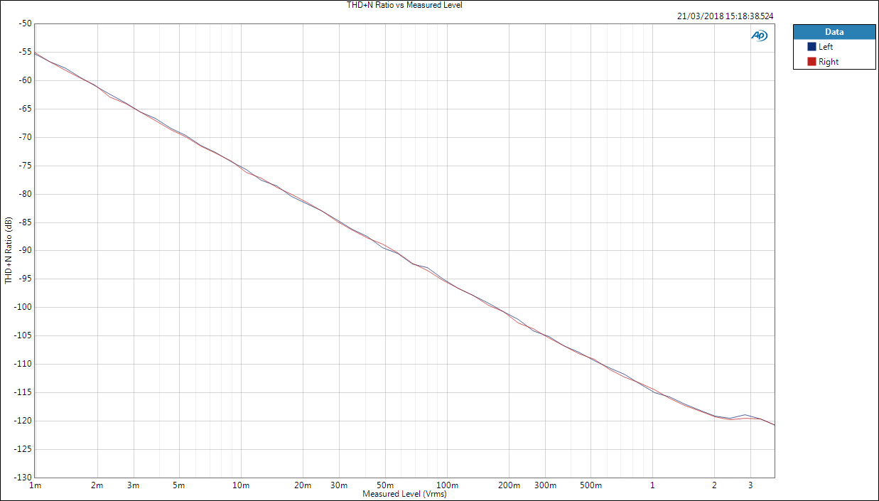
B-version THD+N ratio vs. output level
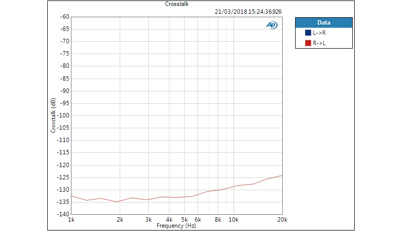
Crosstalk
To be honest I was a bit suspicious about crosstalk figures as they are so low. Opamps are shared between channels so it really should not be this low but I have tried to measure it several times and always get similar results so I do not know what could cause this. Nevertheless, crosstalk can be considered superb.
A-version
With inverted opamp, 6 dB gain.

A-version crosstalk
B-version
Without inverting opamp, 0 dB gain.
B-version crosstalk
Files
- v2.0 PCB files
- v2.0A files
- Schematics
- BOM
- May not be perfect, check carefully if making order based on BOM
- Prices are in GBP, without VAT, and not up-to-date
- v2.0B files
- Schematics
- BOM
- May not be perfect, check carefully if making order based on BOM
- Prices are in GBP, without VAT, and not up-to-date
References and additional information
Version history
Schematics / PCB version history and known errors and bugs
- v1.0A Initial version
- v2.0; major changes in the design compared to v1.0:
- Still supports H-DAC
- Easier to use outside H-DAC
- No filter components
- Separate input pinheaders
- Mounting holes
- Normal opamps instead of fully differential opamp
- Reference designators on silkscreen
- 2-layer board, slightly larger than v1.0A
- Two population options:
- v2.0A: dual opamp design
- v2.0B: simpler single opamp design
This page version history
- 9.4.2018 Initial version
- 5.9.2018 Corrected few mistakes in the text and added simplified schematics