
Amplifier daughterboard for HP MoBo modular headphone amplifier
- TPA6120A2-based simple-IC headphone amplifier amplifier
- Balanced input, balanced output
- Jumper link for extra gain option; default 0/10 dB
- SNR: 116-122 dB A-w depending on the gain and load combination
- THD+N ratio at 100 mW
- 300 Ω: 0.0015 % / -96 dB
- 32 Ω: 0.006 % / -84 dB
- 16 Ω: 0.009 % / -81 dB
- Max power around 0.5 W (16 / 32 Ω)
HP TPA is a simple headphone amp based on TPA6210A2 IC and was used to prove the modular headphone amplifier concept. Despite its simplicity, it offers solid performance for both low-impedance and high-impedance headphones.
Design and schematics
This board is not a complete on its own but is to be stacked on HP MoBo board that contains connectors and power distribution.
This is a very simple design, more like to prove the concept of the modular headphone amplifier. As TPA6210A2 is basically a high-power (current-feedback) operational amplifier, thus the circuit is like an opamp buffer.
TPA6210A2 is a dual-amp chip but to still create balanced output a ground lead from feedback point is taken as cold wire. Despite only hot wire is driven, this is a proper balanced output and gives the benefits of balanced interconnection. There is slight impedance imbalance due to amplifier output impedance but it is negligible when high 10 Ω output resistors are used.
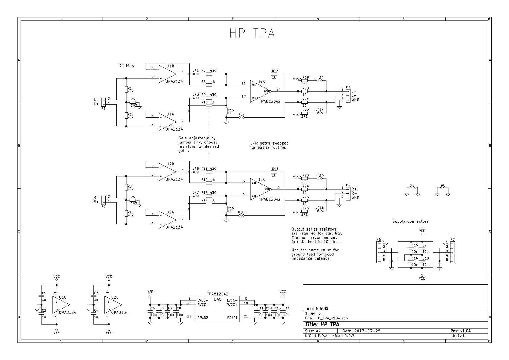
HP_TPA schematics
A pair of OPA2134s is used for input buffering and to keep the input impedance high for good signal balancing. 47k resistors keep the differential input impedance reasonable, while 2M2 lifts common-mode impedance really high. The latter ensures high common-mode rejection but if only very high resistors to ground in each input were be used, opamp input differences and parasitics would cause input impedance (namely the reactive part) imbalance. It is also worth noticing that HP Mobo contains input RF-filter components which significantly reduce the common-mode rejection at higher frequencies.
Note that OPA2134 is a FET-input opamp and therefore has very low input bias current (typical 5 pA). Bias current drawn through very high 2M2 resistor will cause common-mode DC level (which does not really matter) and difference between input currents (= input offset current) through 47k resistors may cause DC offset at the output. These currents in FET-opamp are almost unmeasurably low but in BJT-opamp the case could be different. At least something to check if changing opamp models.
There are two selection points by jumper links: gain can be set to 0 dB or around 10 dB (430 in parallel with 1k), and output impedance can be set to 10 ohms or 1.8 ohms with shown resistors. TPA6210A2 datasheet recommends at least 10 ohms for stability but generally we want as low as possible. This leaves some room for easy experimentations. Note that output resistors are placed both in hot and cold (ground) outputs for proper balanced interconnection.
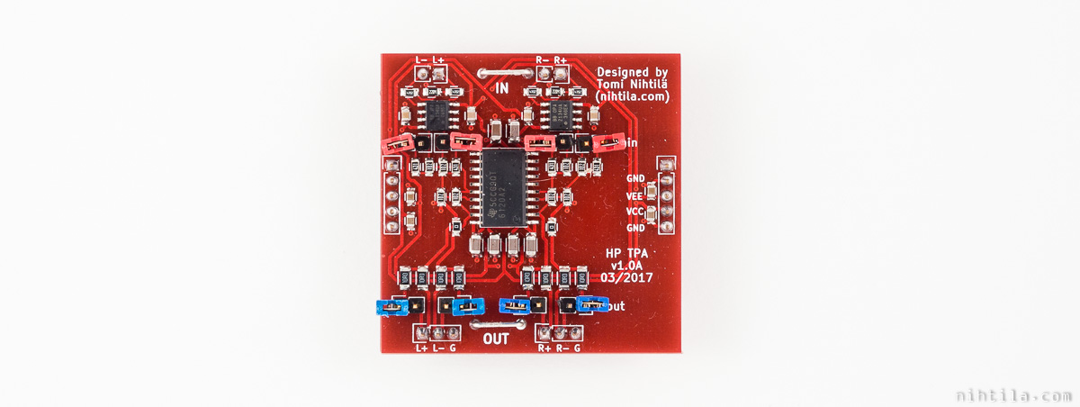
Populated PCB top
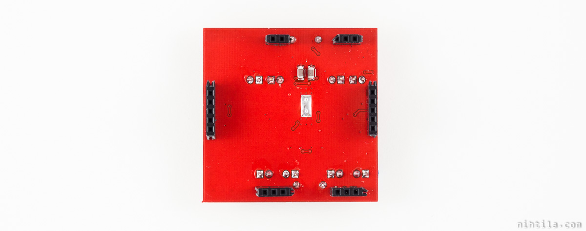
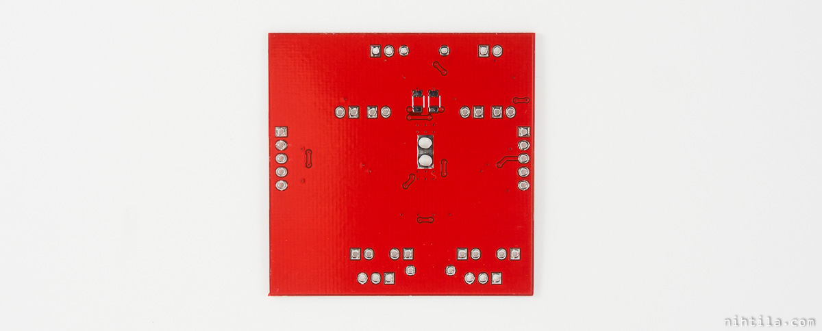
Populated PCB bottom
Layout
This is a 5×5 cm relatively straightforward 2-layer board.
There are two holes provided for TPA6210A2 thermal pad. This way it is possible to solder the thermal without hot air, just by using a soldering iron. You just need to heat it a lot and ensure the thermal gets soldered. With this approach I advise soldering the IC before anything else.
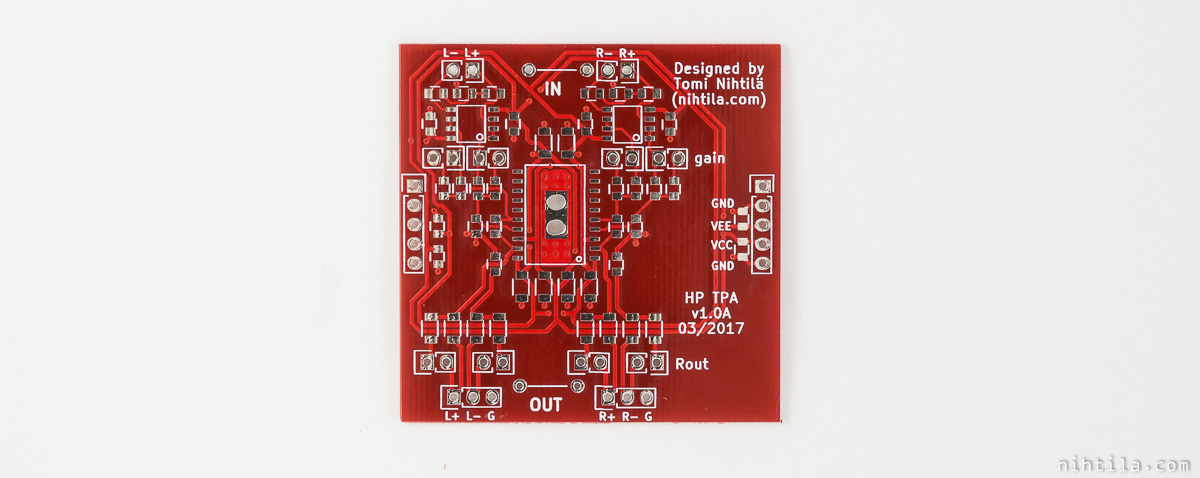
PCB top
PCB bottom
Measurements
I have measured the board at work using Audio Precision APx555 audio analyser. Unless otherwise mentioned, measurement bandwidth is 20 kHz and frequency in single-tone measurements is 1 kHz.
The board is powered by a bench PSU (VD = 7 V, VA = ± 14 V) and loads are resistive.
Output resistor were set to 10 Ω as it is the minimum suggested by TI.
Automated measurement sequences were ran with five different cases:
- 10 dB gain, 300 Ω
- 10 dB gain, 32 Ω
- 10 dB gain, 16 Ω
- 0 dB gain, 32 Ω
- 0 dB gain, 16 Ω
From now on, these cases are referred with numbers 1-5.
Current consumption
Idle current from ±14 V is 36 mA.
In addition to that, HP MoBo mute circuit draws around 50 mA from 7 V digital supply.
Noise floor, signal levels, and SNR
Noise floor here depends not only on gain but also load impedance. Recorded noise floor is
- -104 dBV
- -107 dBV
- -110 dBV
- -112 dBV
- -115 dBV
Datasheet states TPA6120A2 noise to be 0.9 μVrms in audio band with 0 dB gain and 16 Ω load. OPA2134 noise voltage density is 8 nV/√Hz, giving 1.1 μVrms in audio band. Thus on paper the noises are quite similar in magnitude but opamps are main contributors. I did a quick noise analysis in LTspice where TPA6120A2 (model not available) was replaced with an ideal opamp. The results are within 1-2 dB of the noise floor measurements above. While TPA6120A2 is current feedback amplifier and noise adds up slightly differently, this gives an indication noise from opamps and resistors is probably higher than TPA6120A2.
As output series resistor is significant compared to load impedances, it heavily affects overall gain. Therefore, measured gain is
- 9.8 dB
- 6.3 dB
- 3.3 dB
- -4.2 dB
- -7.2 dB
As can be seen, differences in gain match the differences in noise floor.
From these we can derive output signal level when input is 2 Vrms (6 dBV):
- 6.12 V = 15.8 dBV
- 4.13 V = 12.3 dBV
- 2.92 V = 9.3 dBV
- 1.23 V = 1.8 dBV
- 0.87 V = -1.2 dBV
Corresponding output power can be seen in THD+N vs. power graphs below.
Now we can determine SNR by taking difference of the noise floor values and these signal levels, both in dBV, rounded to the nearest dB:
- 120 dB
- 119 dB
- 119 dB
- 114 dB
- 114 dB
Overall, very good numbers. Note that these are non-weighted, A-weighting will add 2-3 dB!
THD+N ratio vs. power
THD+N are swept from 100 mVrms to 2 Vrms input as 2 Vrms seems reasonable maximum input value. For even better numbers one could drive higher signal but it may not be reasonable anymore if no source gives that high level. Even 2 Vrms is quite high for home equipment but it is the default 0 dBFS level of my H-DAC, for example.
10 dB gain setting, 300/32/16 Ω load
300 Ω shows the lowest distortion but also lowest maximum power, as expected. Into 32 Ω and 16 Ω TPA6120A2 has this weird THD+N shape that it first increases and then starts decreasing again, I saw this in Addon H-PreAmp board as well. Maximum output power remains the same with 32 Ω and 16 Ω loads as high output impedance (10 Ω) eats the gain difference. 0.006 % (-84 dB) at 500 mW is quite good number although distortion is higher in lower levels.
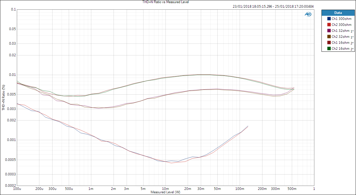
THD+N ratio at 10 dB gain setting
0 dB gain setting, 32/16 Ω load
Here graph shape remains the same but it is shifted. Maximum output power is significantly lower but some smaller power levels have lower THD+N. There are no clear advantages here in using lower gain due to odd distortion profile. As was shown, also SNR is higher with higher gain setting.
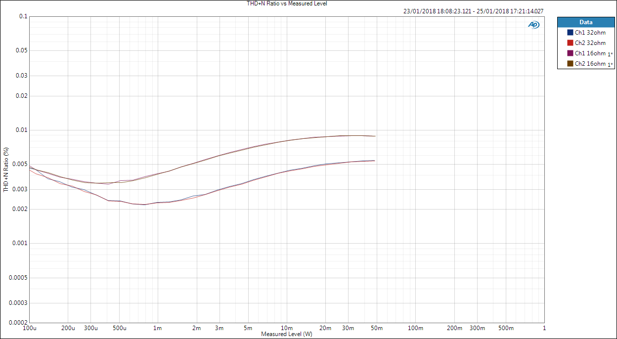
THD+N ratio at 0 dB gain setting
Crosstalk
Crosstalk is good to very good but not superb. Higher frequency crosstalk is quite independent of load and increases 6 dB/octave, an indication of capacitive coupling. Lower frequency crosstalk gets worse when load current increases. I do not understand exactly why it is lower in between but this is almost identical to TPA6120A datasheet graph so crosstalk is limited by the IC itself. At least it is the lowest in range of frequencies our hearing is the most sensitive.
Note that this is using balanced output on HP MoBo, otherwise crosstalk is poor.
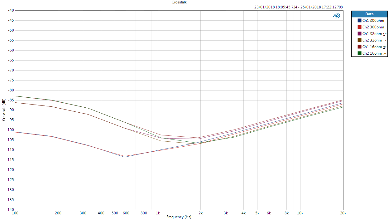
Crosstalk, 10 dB gain setting
Conclusion
TPA6120A2 performance is solid but not exceptional. I have not measured other single-IC headphone amplifiers but I have understood that it is exceptional in its category, hence very easy way to create a good headphone amp.
We could probably get higher SNR by using better opamp buffers. Datasheet claims 128 dB SNR; compared to numbers here one must consider at least weighting filter and used signal level – SNR figures can be boosted by using higher signal level if noise remains the same.
THD+N figures are significantly weaker than in datasheet. I cannot guess what could be the reason for that. I have measured similar numbers in Addon H-PreAmp. It is unlikely I will do more investigation on this as I already have better amplifier modules (HP Buf).
One big question is also the recommended high (minimum) output impedance of 10 Ω. Datasheet clearly states we should not go lower than that – of course we could try but it can lead to instabilities. Amplifier output impedance should be an order of magnitude lower than load impedance to not cause frequency response alteration or reduced damping. NwAvGuy has written excellent post regarding these impedances. It would be interesting to measure headphone frequency responses using different amps.
Files
- v1.0A files
- Schematics
- Component placement top
- Component placement bottom
- BOM
- May not be perfect, check carefully if making order based on BOM
- Prices are in GBP, without VAT, and not up-to-date
References and additional information
- HP MoBo motherboard for this amplifier module
- TPA6120A2 datasheet
- OPA2134 datasheet
- NwAvGuy – Headphone & Amp Impedance
Version history
Schematics / PCB version history and known errors and bugs
- v1.0A Initial version
This page version history
- 4.2.2018 Initial version