
Motherboard for modular headphone amplifier system
- Motherboard with inputs, outputs, power distribution, and signal routing for amplifier daughterboard
- Balanced input
- Balanced and unbalanced outputs
- Output mute circuit
- Requires separate amplifier board
HP MoBo is the basis of a modular headphone amplifier design. It provides input and output connections and simple power supply components (external power supply required), and connections for stackable amplifier daughterboard.
This allows for easy and cost-effective experimentation of various amplifier circuits as the daughterboards are only 50 mm x 50-70 mm and without bulky connectors. Currently there are two amplifier daughterboards available: HP TPA and HP Buf, the latter with two buffer options.
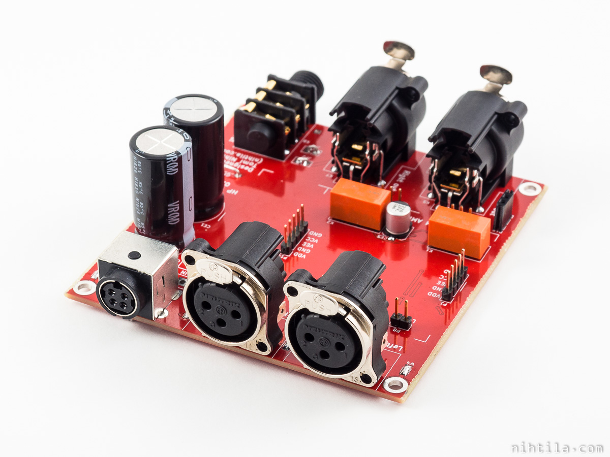
Power and input connectors; it is designed to be used with my DIY power supply
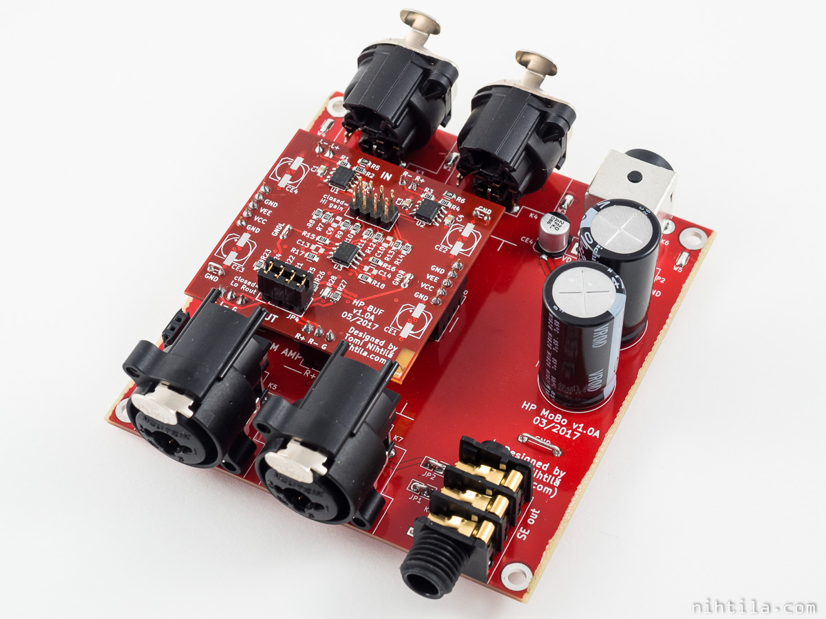
HP Buf stacked on HP MoBo
Design and schematics
HP MoBo has rather unusual HP amp approach as it does not contain volume control and has only one input – think of it as a power amplifier similar to speaker systems. This is designed for my own needs, it will be part of a system that already includes a separate preamplifier with volume control. This way it is simpler to replace one component in the system.
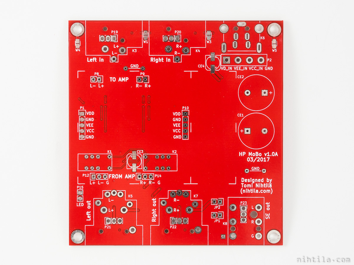
Audio connections
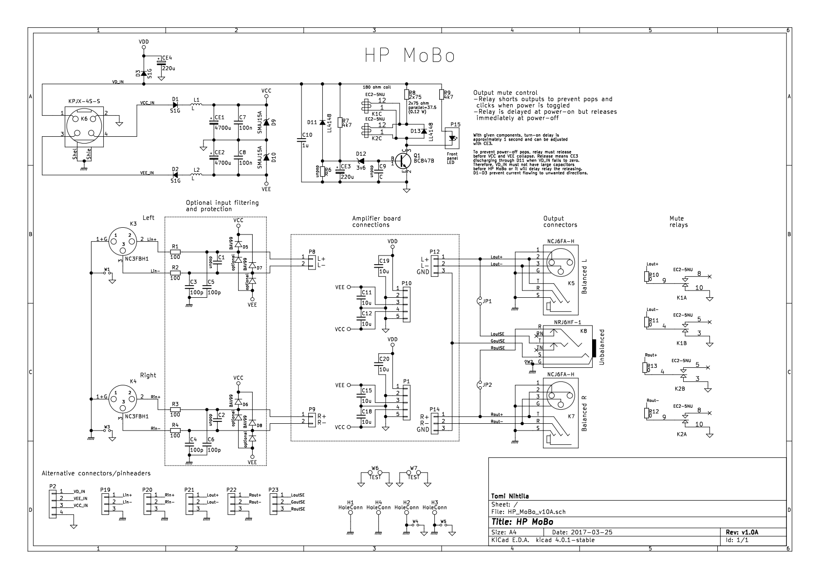
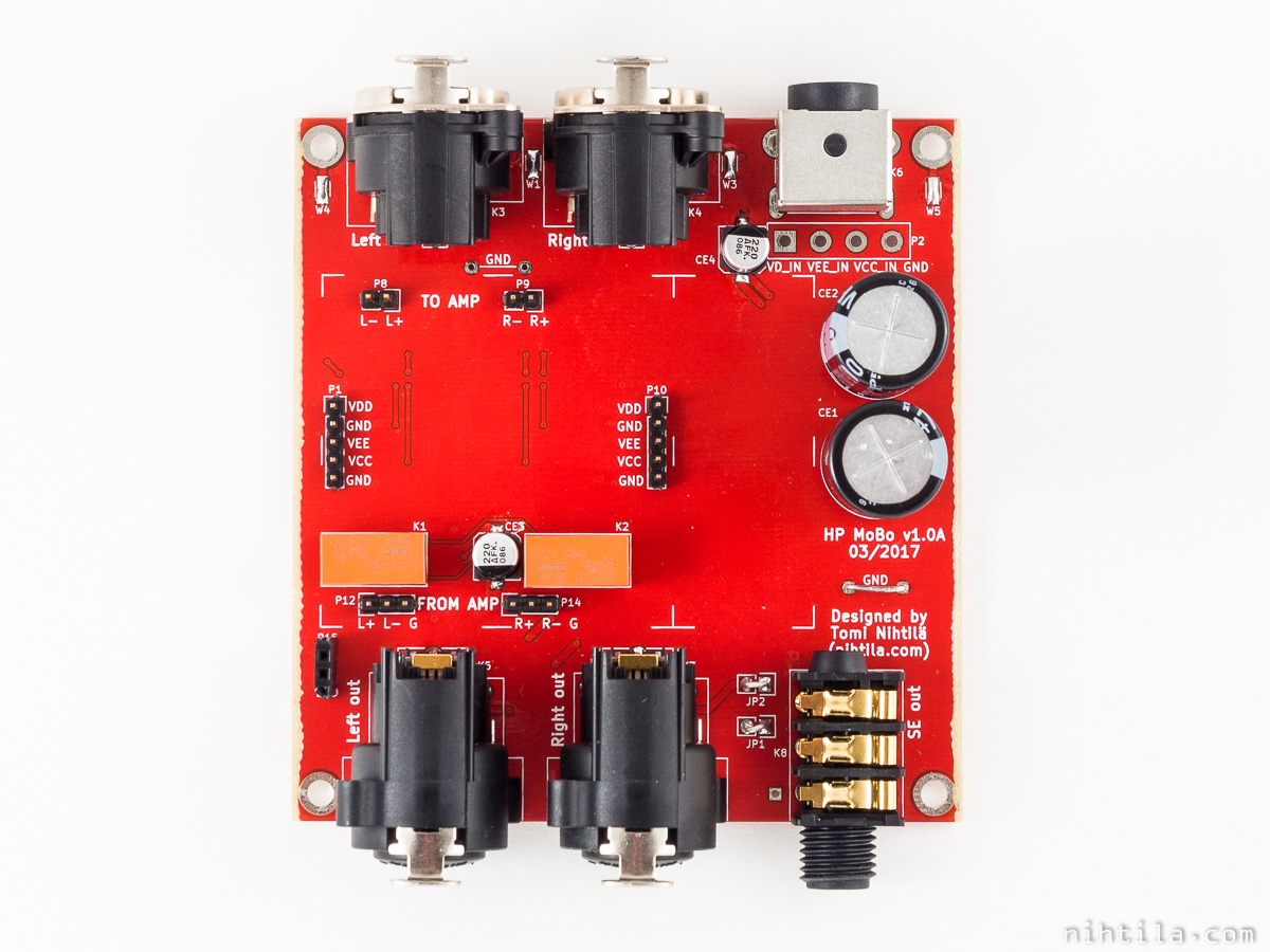
Signals comes in via K3 and K4. 100 ohm resistors and 100 pF capacitors provide some input RF filtering and optional protection diodes can be populated. P8 and P9 take input signal to an amplifier daughterboard.
Amplified balanced signal returns via P12 and P14. This signal is routed directly to the output connectors which are Neutrik combo type, accepting both XLR and 6.3 mm 3-pole plug. These are meant for balanced headphones. Balanced interconnects are usually available only in high-end headphones and even there 4-pin XLR is more common than two 3-pin XLRs. But as this is DIY and so will be the headphone cables, I wanted to keep these separate. Note that when XLR is used for headphones, gender is diversed compared to normal XLR interconnections – headphone output connectors are female. This is the same convention used in headphone amplifiers with XLR outputs.
For common unbalanced headphones, traditional 6.3 mm socket K8 is provided. This takes positive signal (hot) of the balanced differential output along with ground wire from the amplifier board. Therefore, voltage swing is half of the balanced signal.
As the amps use balanced inputs, it is desirable to have balanced impedance in amplifier boards. Although probably negligible, it is worth understanding that RF protection components on inputs (100 ohm resistors and 100 pF capacitors) will become part of this input impedance and cause impedance imbalance at high frequencies.
Mute circuit
Output relays K1 and K2 prevent pops and clicks when powering up and down the device. By default, outputs are shorted to ground via the relays. For balanced connection, one relay shorting positive and negative outputs would have been enough. However, to ensure pop-free operation on single-ended headphone jack I used two relays to short all four output leads to ground.
There are placeholders for series resistors if direct short to ground is unwanted. However, the effectiveness of mute depends on the amplifier board output impedance and the resistance of these mute paths. When I was testing these with amplifier of near-zero output impedance, the output did not mute completely even with 0-ohm resistors. This is due to the fact that these small relays still have relatively high contact resistance compared to near-zero-ohm amplifier output impedance. This is a simple voltage divider. But most importantly, there was no pops and clicks when toggling the power of the amp so the circuit still does its job. I did not want to put the audio through closing relay contact as this would add extra resistance and parasitics in the signal path.
Relays are controlled by a separate circuit. After power-up, the relays turn on after a delay. When power is turned off, the relays will release immediately. With given components, turn-on delay is approximately R7*CE3, meaning one second with shown component values. It is assumed that VDD is 7V as is in my external power supply.
CE3 charges through R7 and when the voltage of CE3 reaches approximately 4.3 V (zener voltage plus Q1 BE junction), D12 conducts. After that the current flowing through R7 goes to Q1 and keeps it open.
When power is turned off, VD_IN decreases rapidly as there are no large capacitors. CE3 is discharged through D11, closing Q1 and turning the relay off avoiding audible pops and clicks. This on relies on VD_IN collapsing faster than it takes the main VCC/VEE reservoir capacitors CE1/CE2 voltage to drop too much to cause glitches on audio output. Therefore, there must not be large capacitors on VD_IN – not on this device nor any other device supplied by the same power supply! Diodes D1-D3 prevent current from flowing to unwanted directions.
Power supply
This is meant to be used with my external PSU providing ±14 V for analog and 7 V for digital. Therefore, this board only has diode protection against polarity, over-voltage protection, and filter capacitors.
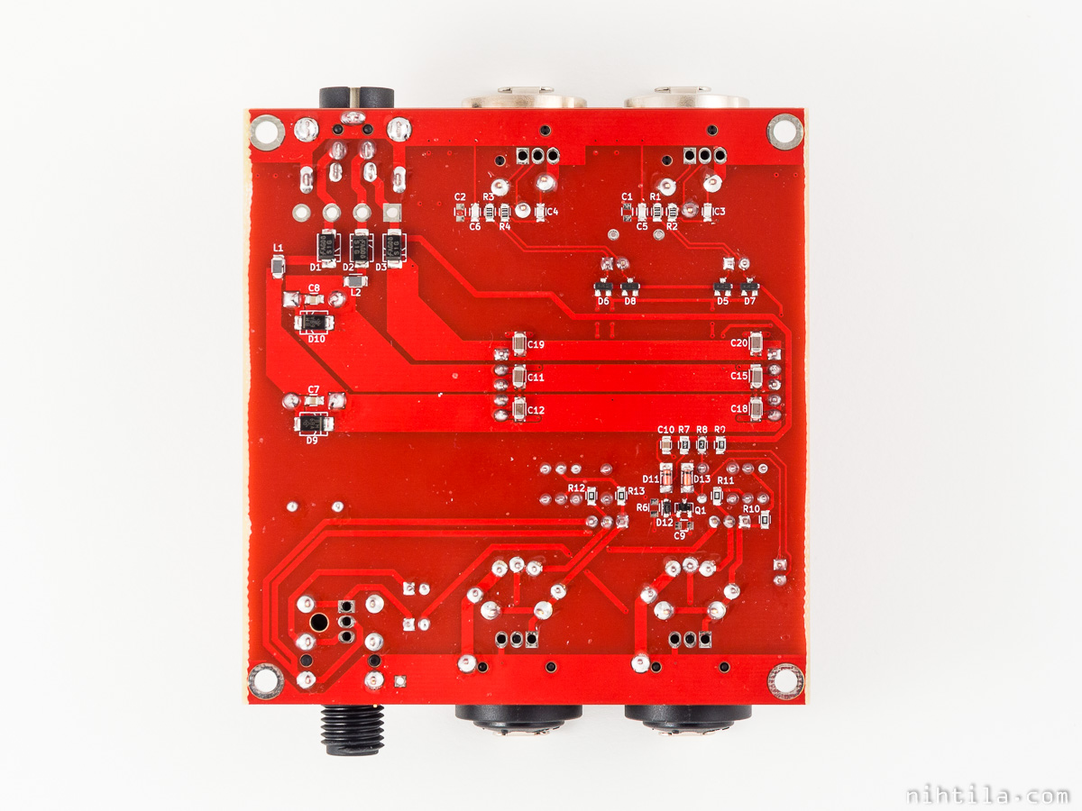
Populated PCB top
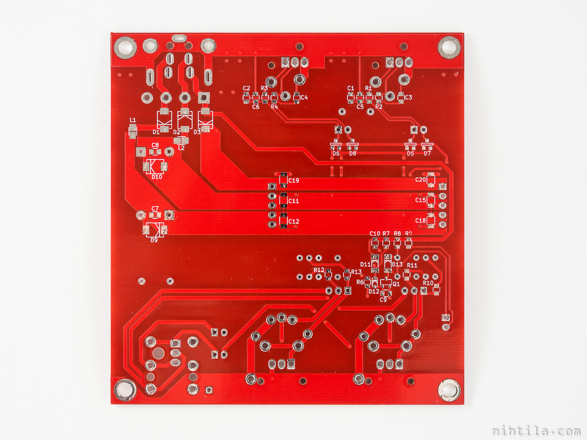
Populated PCB bottom
PCB edges are scraped to fit the enclosure tracks.
Layout
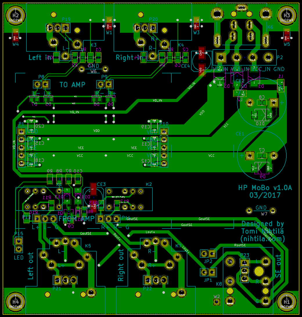
PCB layout is very simple as the board has plenty of space and only few signals. The two layers are swapped compared to common convention, ground plane on top and signals on bottom side. This gives some extra shielding when amplifier boards are stacked on top.
All connectors are PCB-mounted to allow neat placement in a fitting enclosure. PCB size is 10×10 cm. The power connector I use is for my external DIY power supply but screw terminal or wires can be mounted as well.
PCBs are from Elecrow.
PCB top (ground)
PCB bottom (signals)

Amplifier boards
Currently there are two amplifier boards from which one can be populated with two different buffers, giving three amplifier options:
- HP TPA – TPA6120A2-based simple single-IC based amplifier
- HP Buf – Opamp circuit with high-current buffer with two buffer options:
- BUF634
- LME49600
Measurements
As this is only part of a system, amplifier performance measurements can be found in the corresponding amplifier board posts. This board has generous clearance between left and right channels so crosstalk here is not an issue.
As was already mentioned in schematics, mute effectiveness depends on the used amplifier board (and mute series resistors). When amplifier has near-zero output impedance, the output does not mute completely even with 0-ohm series resistors. This is due to the fact that these small relays still have relatively large contact resistance compared to near-zero-ohm amplifier output impedance. This is a simple voltage divider. But most importantly, there was no pops and clicks when toggling the power of the amp so the circuit still does its job.
Mute delay is approximately 1 second with default component values.
Files
- v1.0A files
- Schematics
- Component placement top
- Component placement bottom
- BOM
- May not be perfect, check carefully if making order based on BOM
- Prices are in GBP, without VAT, and not up-to-date
Related boards and devices
- Amplifier boards:
- Encased device containing this board and an amplifier board:
- Modular HP Amp
Version history
Schematics / PCB version history and known errors and bugs
- v1.0A Initial version
- Mute circuit does not mute perfectly if amplifier output impedance is near-zero due to quite high relay contact resistance; however, as it still suppresses pops and clicks, I have no intention to change this.
This page version history
- 04.2.2018 Initial version