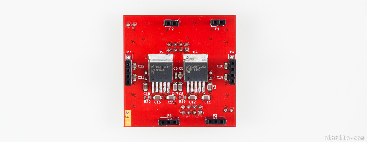
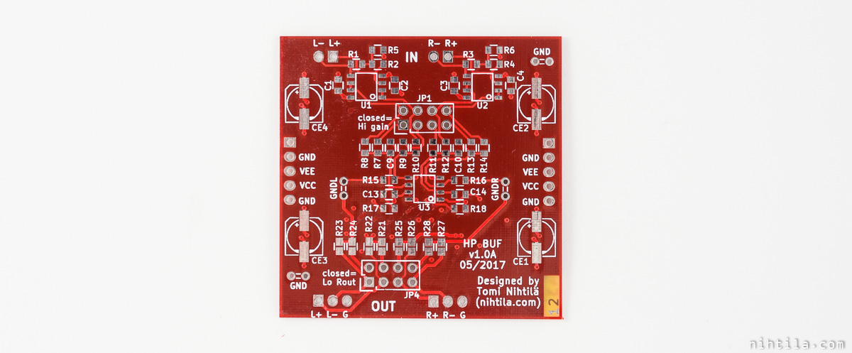
Amplifier daughterboard for HP MoBo modular headphone amplifier
- High-power high-performance balanced headphone amplifier daughterboard for HP MoBo
- Balanced input, balanced output
- Jumper link for two gain options, default 0/10 dB
- Jumper link for two output impedance options
- OPA2134 opamps followed by BUF634 or LME49600 buffers
- SNR: 113-121 dB A-w depending on the buffer, load, and gain
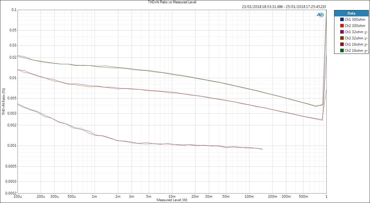
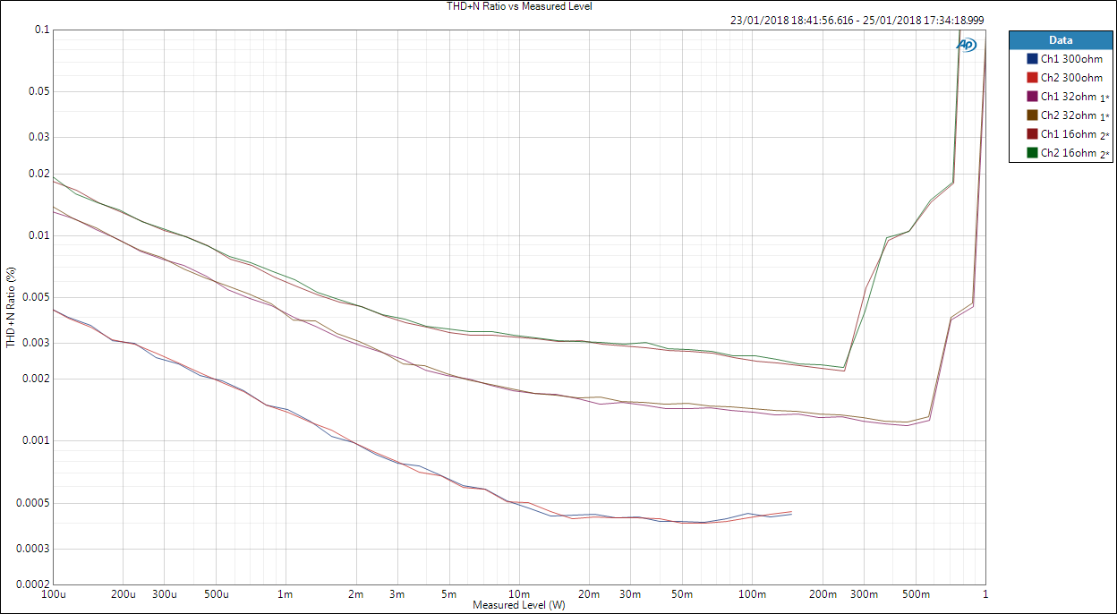
- THD+N ratio at 100 mW (LME49600)
- 300 Ω: 0.0004 % / -108 dB
- 32 Ω: 0.0007 % / -103 dB
- 16 Ω: 0.0012 % / -98 dB
- Max power around 1 W (<0.1 % THD+N)
- Update: get even higher performance with LM4562 opamps
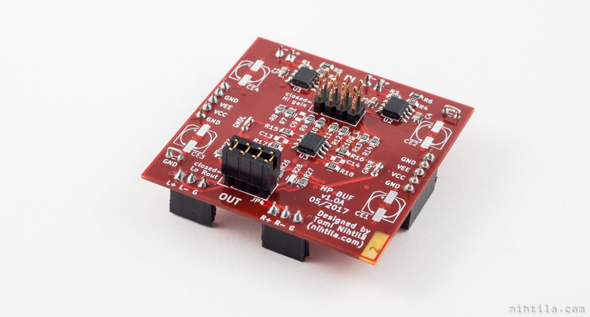
HP Buf is an amplifier daughterboard for HP MoBo modular headphone amplifier. It offers high output power into any load, balanced operation, and very high performance figures. By 4-layer PCB design, the amplifier is very compact yet provides efficient heat conduction for the buffers.
Design and schematics
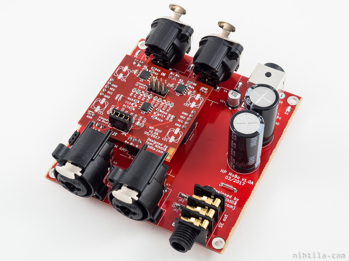
This board is not a complete on its own but is to be stacked on HP MoBo board that contains connectors and power distribution.
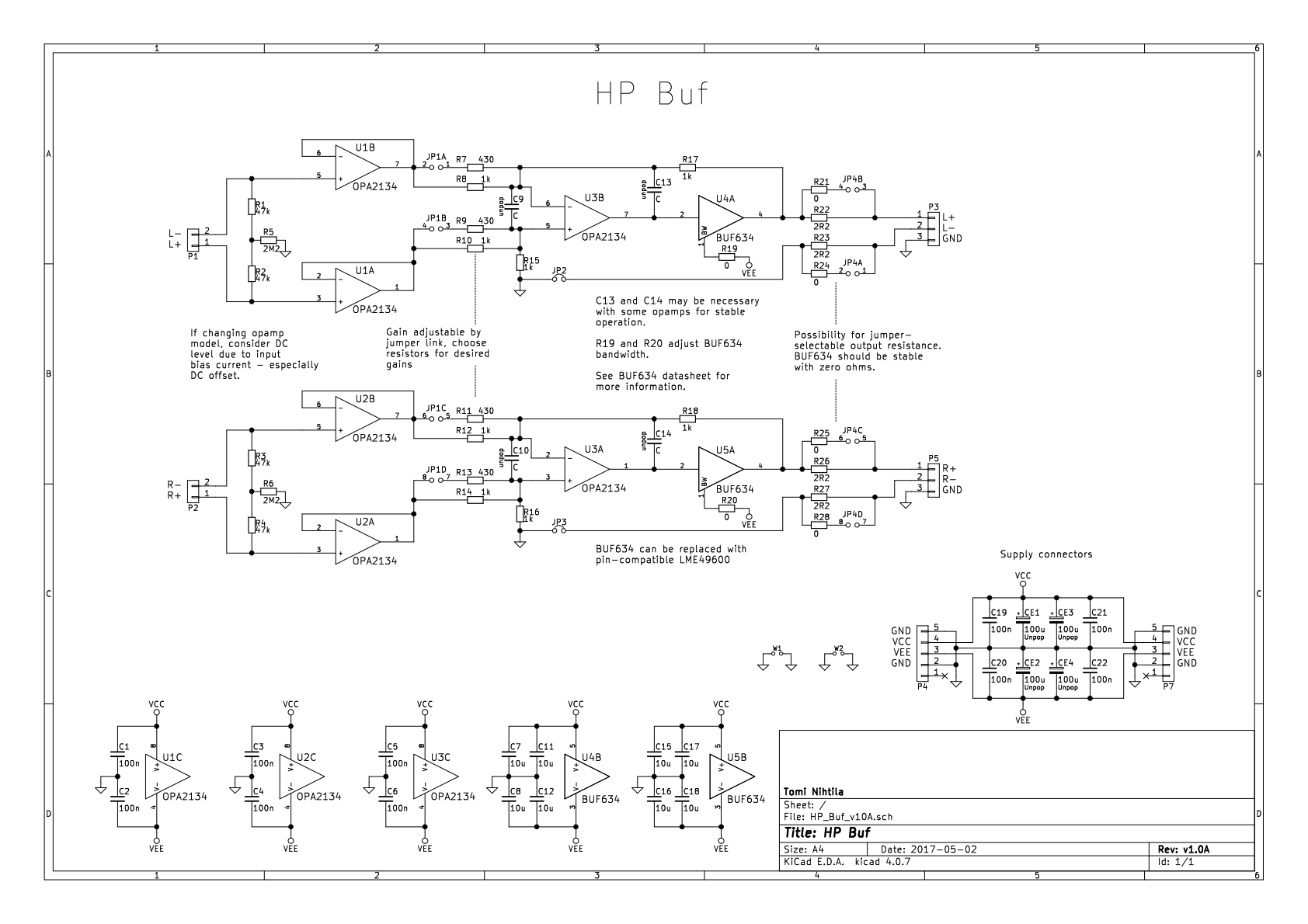
A pair of OPA2134s is used for input buffering and to keep the input impedance high for good signal balancing. 47k resistors keep the differential input impedance reasonable, while 2M2 lifts common-mode impedance really high. The latter ensures high common-mode rejection but if only very high resistors to ground in each input were be used, opamp input differences and parasitics would cause input impedance (namely the reactive part) imbalance. It is also worth noticing that HP Mobo contains input RF-filter components which significantly reduce the common-mode rejection at higher frequencies.
Note that OPA2134 is a FET-input opamp and therefore has very low input bias current (typical 5 pA). Bias current drawn through very high 2M2 resistor will cause common-mode DC level (which does not really matter) and difference between input currents (= input offset current) through 47k resistors may cause DC offset at the output. These currents in FET-opamp are almost unmeasurably low but in BJT-opamp the case could be different. At least something to check if changing opamp models. It is only the differential DC level that matters, any common-mode DC will stay at the differential amplifier U3.
Update: offset is not a problem with BJT-input LM4562 either.
After the input buffers are OPA2134 as differential amplifier and BUF634 buffer inside the feedback loop. There are placeholders for capacitors (marked unpop) that may be required with some operational amplifiers, see BUF634 datasheet for more information.
There are two selection points by jumper links: gain can be set to 0 dB or around 10 dB (430 in parallel with 1k), and output impedance can be set to 0 or 2.2 ohms – or whatever resistors populated. There are no output series resistors in BUF634 datasheet so it should work with zero resistance. For better stability, small resistors (few ohms) can be added but in general the lower the better.
Instead of actively driving both hot and cold wires, one buffer per channel is used but to create balanced output a ground lead from feedback point is taken as cold wire. When impedance of both leads are identical, this is a balanced connection with all benefits. It is not necessary to drive both sides actively. There is slight impedance imbalance due to amplifier output impedance though but it should be close to zero.
BUF634 can be replaced with LME49600 as they are similar and have identical pinout.
There are plenty of power supply decoupling caps but they may not be all necessary at least when used with HP Mobo which has large caps at close proximity. I have not populated the 100u elcos in my prototype board.
Layout
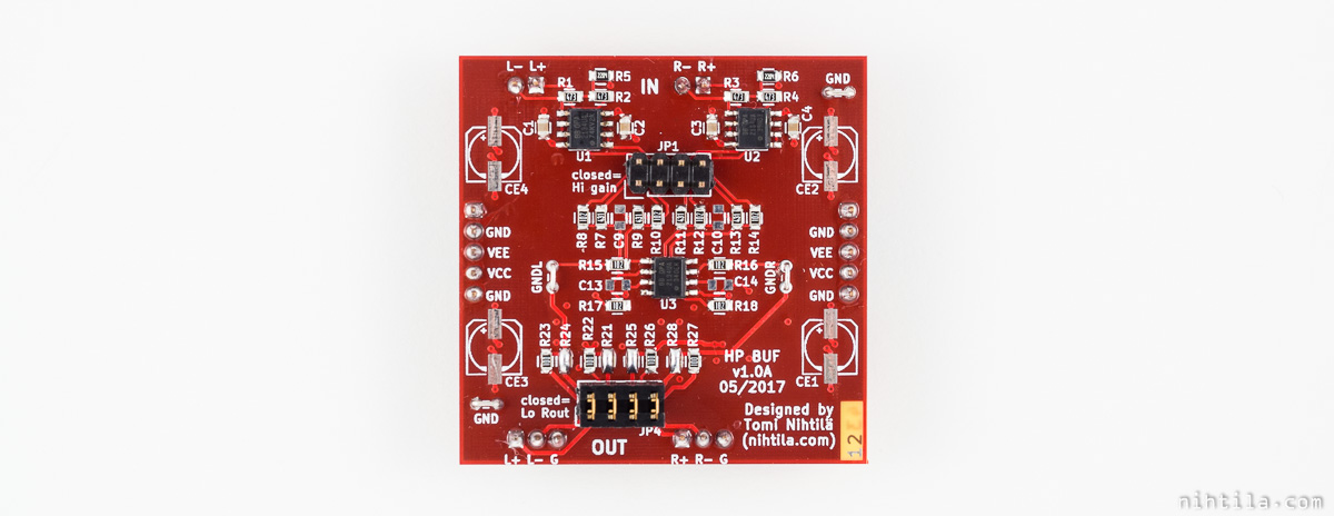
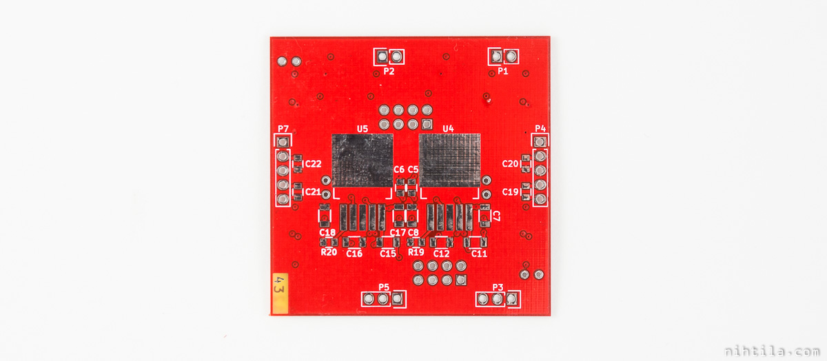
PCB layout is 4-layer design to keep it compact and neat. As the design is very straightforward, all signals are on top layer. Layer stackup is signal, GND, VCC, VEE because signals are only on top and BUF634/LME49600 thermal tab is connected to the VEE pin. This makes the bottom layer effectively a heatsink; this would be better on top but I still wanted to have the signals and components on top layer.
PCBs are from Elecrow where even (small) 4-layer boards are very cheap.
Measurements
I have measured the board at work using Audio Precision APx555 audio analyser. Unless otherwise mentioned, measurement bandwidth is 20 kHz and frequency in single-tone measurements is 1 kHz.
The board is powered by a bench PSU and loads are resistive using a headphone load box.
There are many possible combinations for these measurements due to BUF634 or LME49600 used, 0 or 10 dB gain, and high or low output impedance. These are all measured with no output series resistor, therefore near-zero output impedance. This is the most preferred but in some cases could lead to instability due to headphone cable capacitance. However, in datasheet examples no resistors have been used.
Note that 10 dB gain setting is actually slightly higher, around 10.5 dB.
Measurements were performed using balanced outputs on HP MoBo. Unbalanced output would lead to poor crosstalk.
Current consumption
Idle current from ±14 V:
- BUF634: 28 mA
- LME49600: 40 mA
In addition to that, HP MoBo mute circuit draws around 50 mA from 7 V digital supply.
Noise floor, signal levels, and SNR – BUF634
Noise floor with different gains (no difference between loads):
- 10 dB gain: -103 dBV / -105 dBV A-weighted
- 0 dB gain: -110 dBV / -112 dBV A-weighted
When input level is limited to 2 Vrms = 6 dBV, maximum output level is then 16 dBV with 10 dB gain and 6 dBV with 0 dB gain. However, as we will see in THD+N graphs, distortion shoots up after 900 mW in high-gain/high-load combinations. Therefore, this is taken as maximum level in those cases.
Maximum usable output levels in five combinations are as follows:
- 10 dB, 300 Ω: 16 dBV
- 10 dB, 32 Ω: 14.5 dBV
- 10 dB, 16 Ω: 11.5 dBV
- 0 dB, 32 Ω: 6 dBV
- 0 dB, 16 Ω: 6 dBV
These lead to following A-weighted SNR figures:
- 10 dB, 300 Ω: 121 dB
- 10 dB, 32 Ω: 120 dB
- 10 dB, 16 Ω: 117 dB
- 0 dB, 32 Ω: 118 dB
- 0 dB, 16 Ω: 118 dB
Without weighting these are approximately 2 dB lower. Excellent figures overall. 0 dB figures could be further boosted by driving higher signal level in.
Noise floor, signal levels, and SNR – LME49600
Similarly figures are drawn for LME49600.
Noise floor with different gains (no difference between loads):
- 10 dB gain: -103 dBV / -105 dBV A-weighted
- 0 dB gain: -110 dBV / -112 dBV A-weighted
When input level is limited to 2 Vrms = 6 dBV, maximum output level is then 16 dBV with 10 dB gain and 6 dBV with 0 dB gain. However, as we will see in THD+N graphs, distortion shoots up after certain point. I have taken maximum signal level points around 0.01 % distortion: 900 mW into 32 Ω and 400 mW into 16 Ω.
Maximum usable output levels in five combinations are as follows:
- 10 dB, 300 Ω: 16 dBV
- 10 dB, 32 Ω: 14.5 dBV
- 10 dB, 16 Ω: 8 dBV
- 0 dB, 32 Ω: 6 dBV
- 0 dB, 16 Ω: 6 dBV
These lead to following A-weighted SNR figures:
- 10 dB, 300 Ω: 121 dB
- 10 dB, 32 Ω: 120 dB
- 10 dB, 16 Ω: 113 dB
- 0 dB, 32 Ω: 118 dB
- 0 dB, 16 Ω: 118 dB
Without weighting these are approximately 2 dB lower. Excellent figures overall. 0 dB figures could be further boosted by driving higher signal level in.
THD+N vs. power – BUF634
THD+N are swept from 100 mVrms to 2 Vrms input level.
10 dB gain setting, 300/32/16 Ω load
300 Ω shows the lowest distortion, quite flat at 0.001 % = -100 dB. Maximum power is the lowest but adequate for most. If not, more gain can be added.
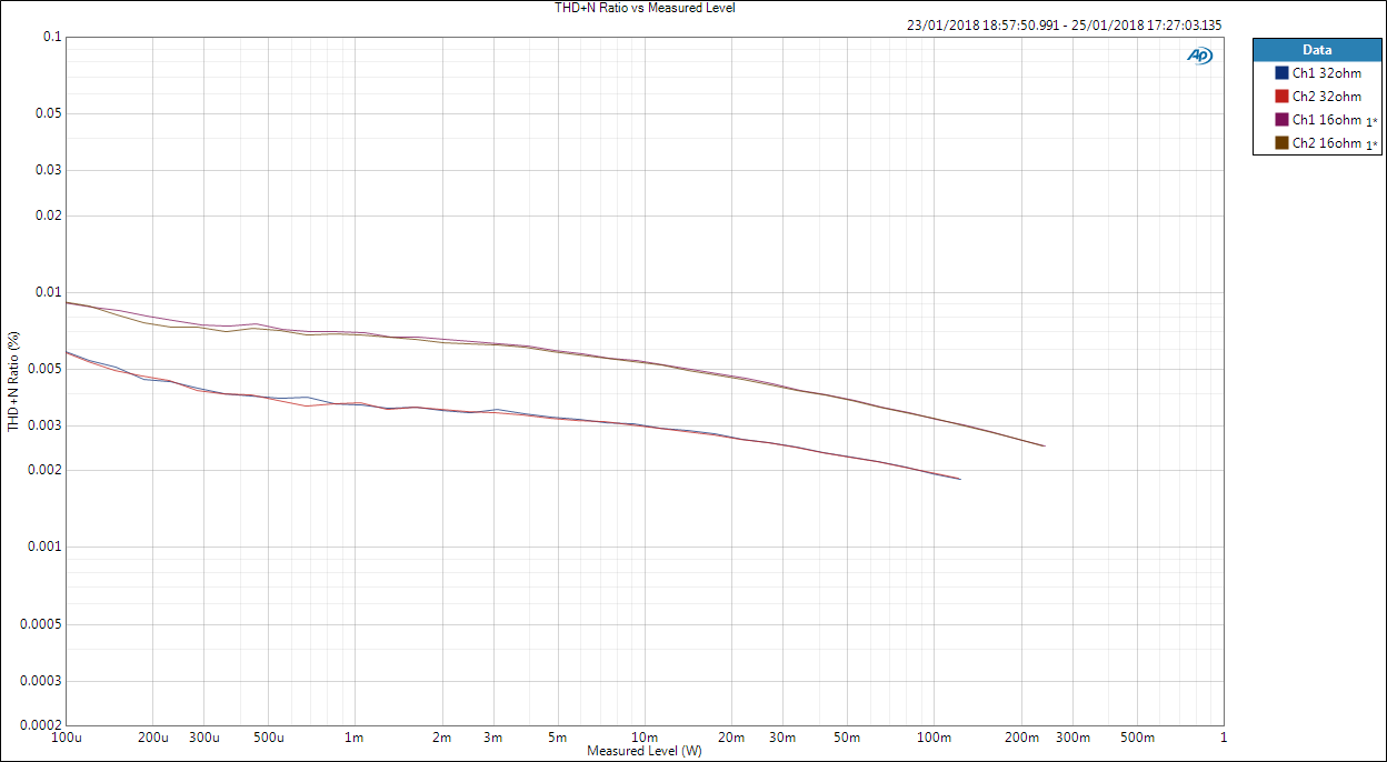
32 Ω and 16 Ω show very good distortion levels especially with higher power. Maximum power is 900 mW at 0.0025 % (-92 dB) and 0.004 (-88 dB) into 32 Ω and 16 Ω, respectively.
0 dB gain setting, 32/16 Ω load
If lower power levels are enough, around 6 dB improvement in THD+N can be achieved by using lower gain.
THD+N vs. power – LME49600
THD+N are swept from 100 mVrms to 2 Vrms input level.
10 dB gain setting, 300/32/16 Ω load
300 Ω shows the lowest distortion, remarkably low 0.0004 % (-108 dB) at higher power levels.
32 Ω and 16 Ω also show excellent distortion levels. Distortion increases rapidly after knee points but one can get 300 mW into 16 Ω or 600 mW into 32 Ω with very low distortion. Lowest distortion near maximum power is 0.0025 % (-92 dB) and 0.0015 % (-96 dB) into 16 Ω and 32 Ω, respectively. Excellent figures.
0 dB gain setting, 32/16 Ω load
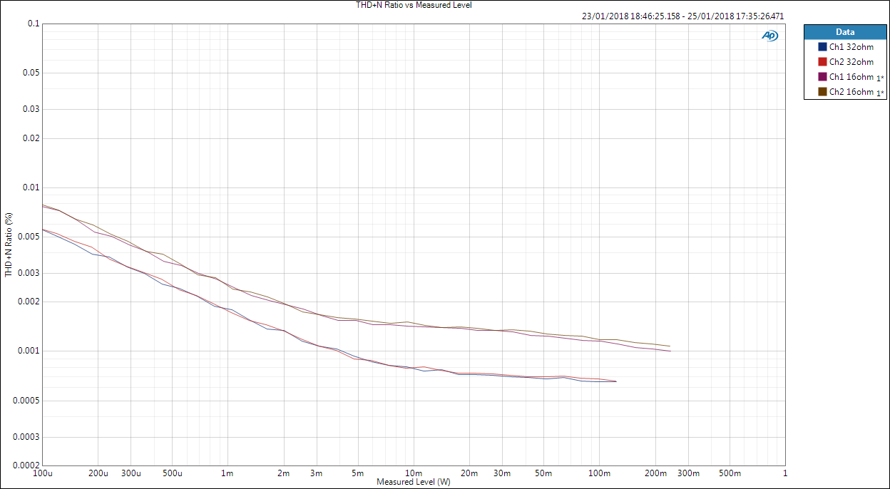
If lower power levels are enough, around 6 dB improvement in THD+N can be achieved by using lower gain, and get even lower distortion levels under 0.001 % / -100 dB with 32 Ω load.
Crosstalk
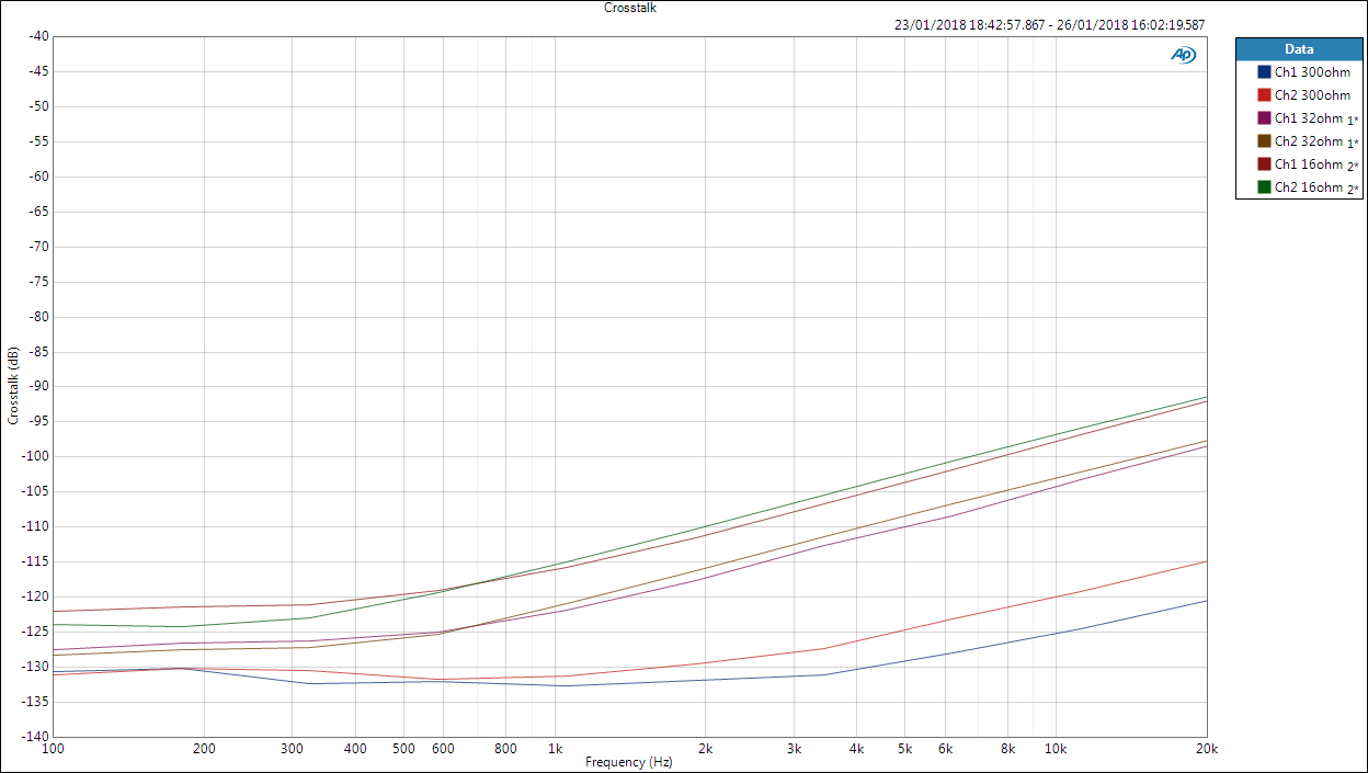
Crosstalk results are very good and identical for both amps. Crosstalk increases with frequency, and higher output current leads to higher crosstalk.
Update 12.2.2018. Crosstalk is likely limited by the headphone dummy load box whose channel separation needs to be improved for future measurements.
BUF634 vs. LME49600
THD+N graphs show LME49600 is a clear winner in terms of distortion. If 100-200 mW maximum power is enough into 32 Ω, gain can be chosen so that THD+N levels of lower than 0.0001 % / -100 dB can be achieved.
Maximum power output is lower in LME49600 than in BUF634.
Measurements vs. datasheets, and conclusions
THD+N figure of 0.000035 % at 0 dB gain, 32 Ω load, and 3 Vrms output is given for LME49600. Extremely low number. So low that it cannot be measured with any commercially available analyser directly, as the datasheet states. I guess that despite very low THD+N measured, something else is restricting the performance. Nevertheless, I am very pleased with the distortion figures with such simple circuit.
BUF634 datasheet has nothing on distortion. Noise voltage density at 10 kHz is 4 nV/√Hz, meaning 0.57 μVrms in audio band (with some assumptions). Corresponding LME49600 noise number is 3 nV/√Hz, meaning 0.42 μVrms. These are very low numbers. It is clear that bottleneck lies elsewhere in the circuit. For example, OPA2134 noise voltage density is 8 nV/√Hz. In fact, I did quick noise analysis on LTspice using otherwise similar circuit but BUF634/LME49600 was missing from the feedback loop. I got noise levels of -113 dBV and -104 dBV for 0 dB and 10 dB gains, respectively. It cannot be a coincidence I have measured almost the same!
What can be seen here, some performance boost could be achieved by changing the opamps to something better, for example LM4562. I will probably do the exercise one day and write another post, although it would have little practical meaning. The figures are extremely good for such a simple circuit anyway. As usually, more important is to adjust circuit gain for optimal output power range to maximise SNR and THD+N. Too often we first attenuate significantly in preamplifier, followed by high gain in power amplifier, discarding good amount of dynamic range.
Update: I tried LM4562 and significant performance boost was achieved.
Files
- v1.0A files
- Schematics
- Component placement top
- Component placement bottom
- BOM
- May not be perfect, check carefully if making order based on BOM
- Prices are in GBP, without VAT, and not up-to-date
References and additional information
- HP MoBo motherboard for this amplifier module
- BUF634 datasheet
- LME49600 datasheet
- OPA2134 datasheet
- Post regarding LM4562 tweak giving huge performance boost
Version history
Schematics / PCB version history and known errors and bugs
- v1.0A Initial version
- All functional but could try LM4562 instead of OPA2134 for lower noise floor.
This page version history
- 4.2.2018 Initial version
- 12.2.2018 Added note of headphone load being the bottleneck in crosstalk measurements and corrected some typos.
- 21.2.2018 Added references to LM4562+LME49600 measurements
