
- Very high performance; measurement results with coaxial S/PDIF input:
- Output level: 2.0 Vrms
- Dynamic range / SNR: 122 dB (A-weighted)
- THD+N ratio: -103 dB (0 dBFS/1 kHz signal, 48 kHz sample rate)
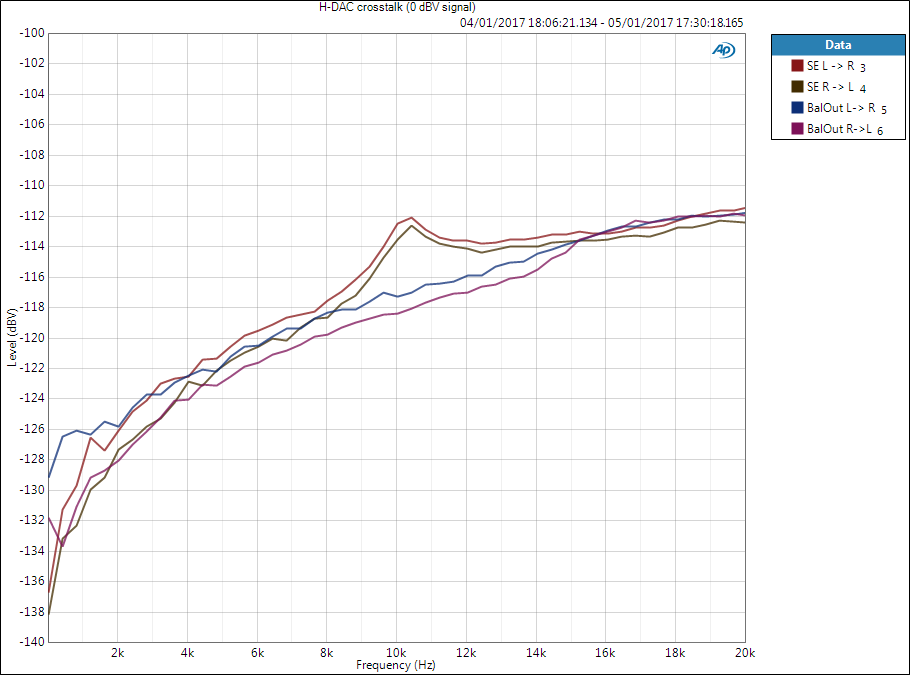
- Crosstalk: -128 dB at 1 kHz, -112 dB at 10 kHz
- Supports S/PDIF, Toslink, USB, and external I2S inputs
- Unbalanced outputs (RCA) on board, balanced (XLR) addon available
- Hardware-controlled – no need for microcontroller (but one can be added with addon)
- Can be powered by AC or DC supply
- Addon available to transform H-DAC into preamplifier/headphone amp
- New output stage addons can be easily designed to experiment with components and circuits
- CS8416 S/PDIF-receiver, PCM1794A DAC, LM4562 opamps (or any SO-8 dual opamp), PCM2707C USB-audio, LM2940/LM2990, TPS73633, TPS79133, and REG103 regulators
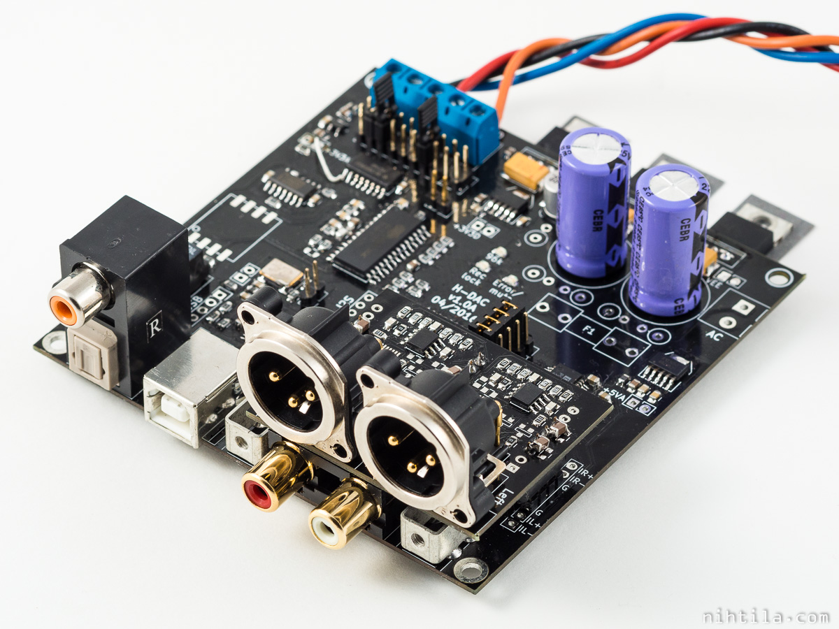
H-DAC is a high-performance 192 kHz / 24-bit capable DAC board with TI PCM1794A DAC. The board has two coaxial S/PDIF, two Toslink, and one I2S input that can be either on-board 48 kHz / 16-bit USB receiver or an external I2S-device. Input selection and settings are controlled with jumper links that can be replaced by mechanical switches or microcontroller addon board.
On-board analog stage is an opamp-based I/V-converter and differential amplifier followed by unbalanced RCA outputs. Addon boards are available to add balanced outputs or volume control and new output stage boards can be designed for addon connectors. Currently available addons are:
- Addon BalOut – Balanced output addon
- Addon H-PreAmp – Preamplifier/headphone amplifier addon
- Addon H-Filter – Simple through-hole balanced preamplifier addon
- Addon H-MCU – Microcontroller addon
Comprehensive audio measurements of H-DAC performance are provided.
H-DAC and Addon BalOut.
Design and schematics
Hierarchically H-DAC consists of four blocks: digital inputs, DAC, analog stage, and power supply. Digital inputs are two coaxial S/PDIF, two Toslink, and one I2S which can be on-board USB or external I2S source. DAC chip has stereo differential current outputs which are low-pass filtered and transformed into single-ended analog voltage outputs in analog stage. PSU supplies numerous voltage rails for analog and digital parts.
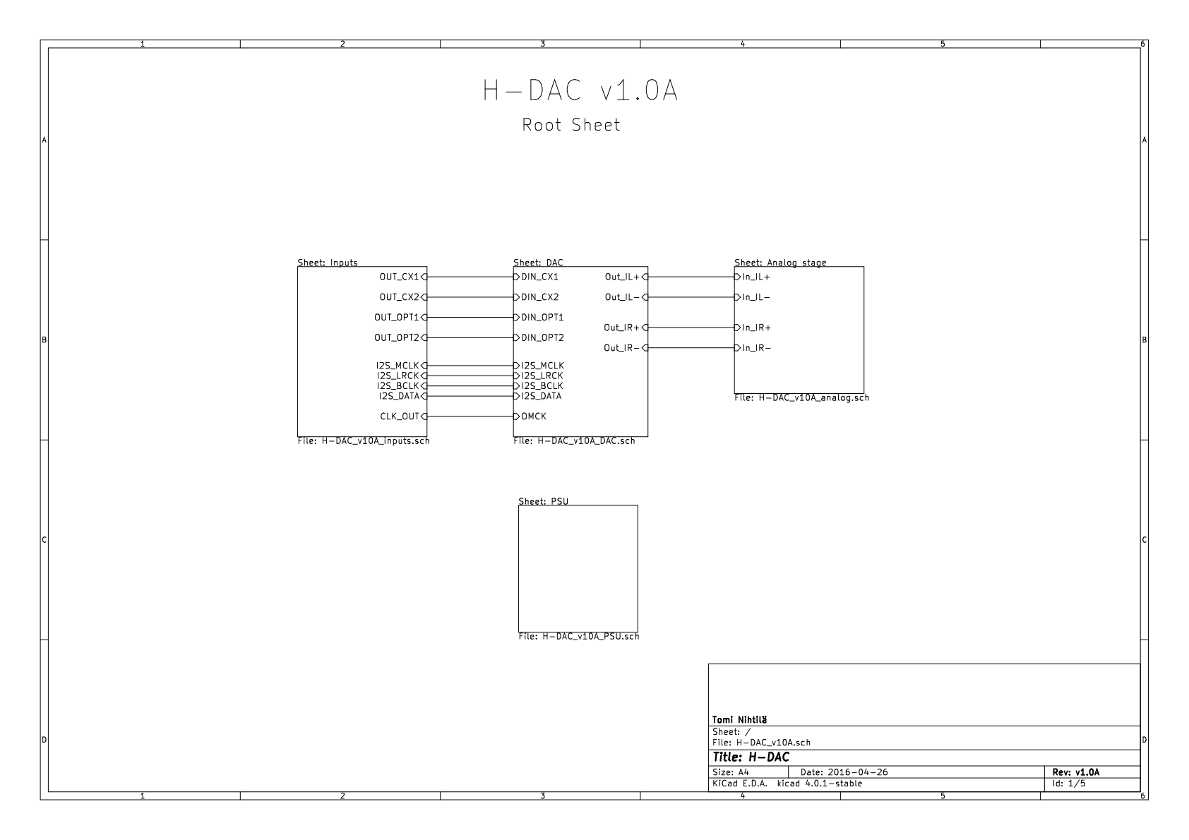
Root schematics (block diagram)
Power supply
Power supply is simple although has plenty of components. It contains only linear regulator circuits but plenty of them as there are separate regulators for opamps (+12/-12 V), 5/3.3 V digital, 5 V DAC analog, and 3.3 V S/PDIF-receiver PLL. H-DAC can be powered from AC-supply or DC-supply (recommended). See the schematics sheet for more details regarding component population.
With AC supply P13 is used followed by rectifier and filtering caps. In this case R25 also connects positive analog supply to digital supply. While separate DC supplies for analog and digital are recommended, the option to use AC wall supply makes it possible to have very small yet high-performance DAC.
External three channel DC PSU with separate supplies for VA+, VA-, and VD connected to P12 is recommended. D1, D12, and D13 are only for polarity protection and can be left out. Input supplies should be externally filtered as there are no placeholders for big capacitors on H-DAC (only C20/C21 for AC operation). Basic regulation is provided by U5, U3, and U4. These are in TO-220 cases and on the edge of the PCB and should be mounted on heatsink or chassis; I like to mount these on chassis to be sure they run cool enough. They can also be slightly picky with the output capacitors which should have ESR of 0.1-1 ohm; I have used 22 uF tantalums but they are quite pricey. The rest of the regulators are surface-mount low-noise types. U6 used for DAC 5 V is high performance regulator but also very expensive – other options may be available. All small pinheaders P14, P15, P16, P18, P19, and P22 are for test purposes only and can be omitted.
While three separate supplies are recommended, VA+ and VD can share positive supply if required by populating R25 which can be a wire or power resistor to take some of the voltage drop from U5 (determine value based on the maximum digital current consumption at 192 kHz sample rate). Note that in case of wire the voltage drop over U5 is quite large and it will get hot if not properly cooled.
Besides the components shown in the power supply sheet, local decoupling capacitors are used close to ICs throughout the board. As cost is not a major design constraint in a hobby project, I have used plenty of capacitors and good regulators.
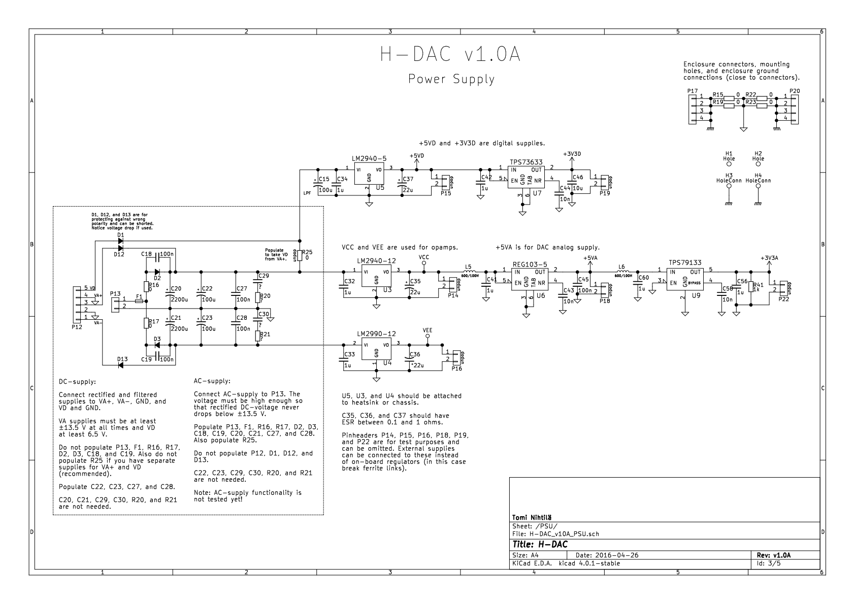
Power supply schematics
Digital inputs
S/PDIF input circuits are pretty standard, more possibilities can be found in the CS8416 datasheet. Toslink/RCA-combo connectors are used which are good for saving PCB space but have turned out to be mechanically not so confident. S/PDIF transformers are used in coaxial paths and level translators in Toslink paths (note that if some Toslinks are not used, the level shifter inputs should be connected to VDD or GND). There is also a BNC-connector footprint on the PCB, and the combo connectors should be replaceable by certain types of Toslink receivers. Wiring connectors out of the board is also possible but keep the leads relatively short and tied together.
There is a tradeoff between ground loop susceptibility and EMC performance. When connectors are totally isolated with transformers, there will not be ground loops but high-frequency interference has easy access to the circuit. Using non-isolated connectors gives good EMC performance but opens path for ground loops. One can first try non-isolated approach and then isolate the connectors if ground loops are problem. Capacitors C3 and C4 are to short high-frequency interference to the enclosure when isolated connectors are used; however, in practice they would need to be directly at the connector to be effective. Anyway, most probably you will not face any issues.
USB-input is pretty much the reference circuit from PCM2707C datasheet – see the datasheet for more information. USB-connector can be placed neatly on-board on provided footprint or wired onto P8 connector. Buffer gate U1B is used to translate 5 V into 3.3 V for D+ pull-up. According to the datasheet, this pull-up should be activated only when USB is connected and device powered up. PCM2707C sends audio out via I2S lines and as this is an oldish part the highest supported audio data format is 48 kHz / 16-bit. For high resolution USB audio, an external USB-to-I2S-converter can be used and connected to P10. If external I2S is used, all PCM2707 circuitry must be left out. When using an external USB device, ensure that signal level is 3.3 V and that clocking schemes are supported by the PCM1794A DAC (which should not be an issue).
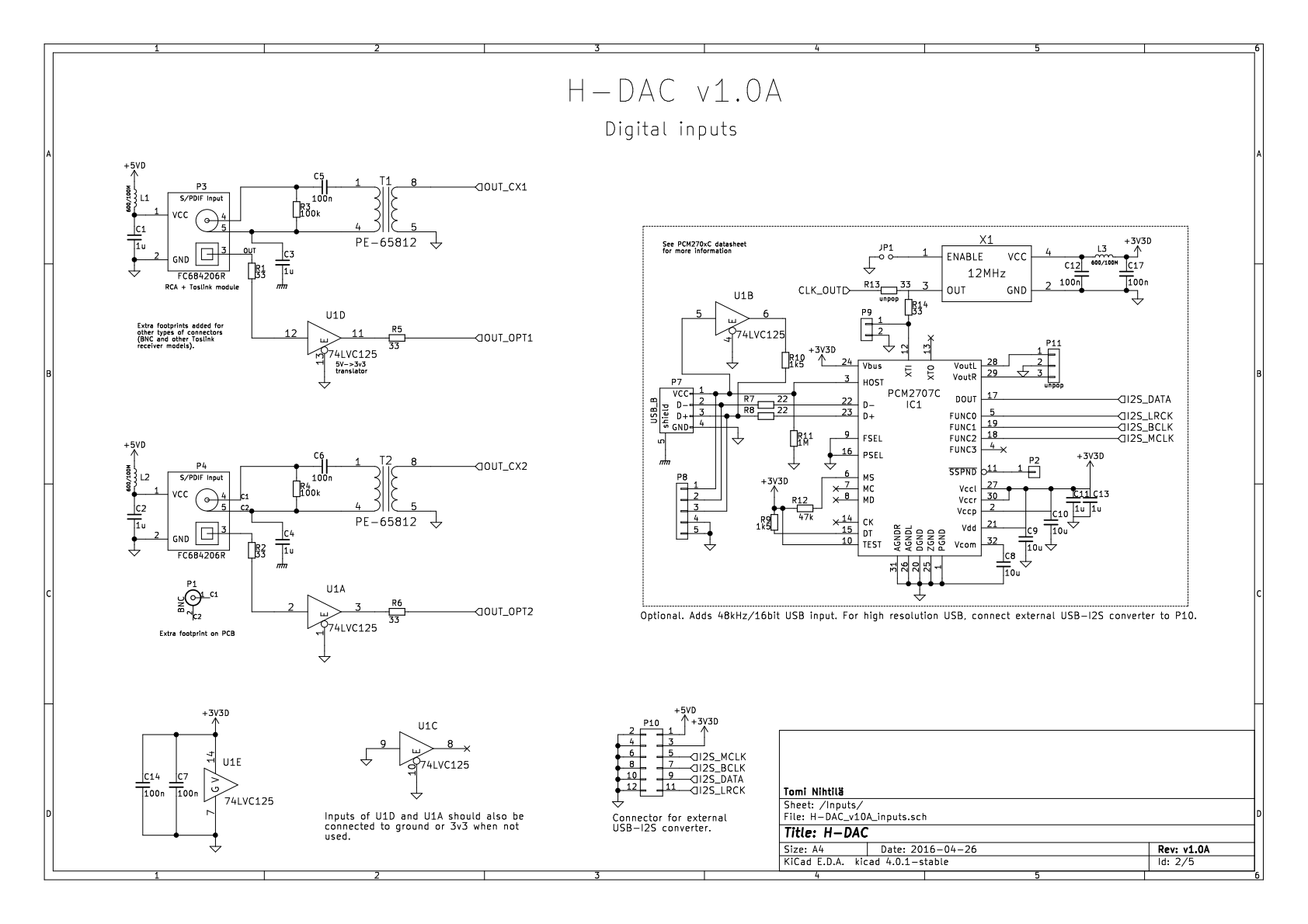
Digital inputs schematics
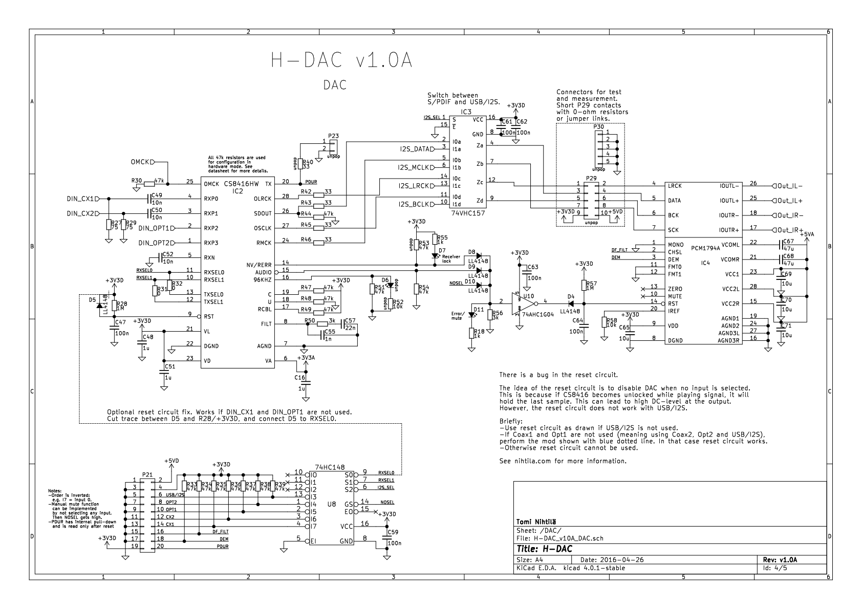
S/PDIF-receiver
Cirrus Logic CS8416 S/PDIF receiver is used. External component functions are explained in the CS8416 datasheet. It is used in hardware-mode here so various 47 k pull-up and pull-down resistors configure the device. Input is selected with RXSEL0 and RXSEL1 signals coming from U8 based on jumper position. There are also LEDs to denote receiver lock or error. Note that LED on 96KHZ pin should denote higher sample rates but it is not working properly, or I do not understand exactly how it works. Therefore, it is not populated.
When CS8416 is locked into incoming S/PDIF signal, it outputs the audio signal in I2S format: OLRCK is the word/frame clock, SDOUT is the data, OSCLK is the bit clock, and RMCK is the master/system clock. These signals are routed to IC3 which is an I2S switch between CS8416 and the external I2S or USB source. P29 and P30 are only for measurement purposes and the P29 contact pairs should be shorted with pieces of wire or 0-ohm resistors.
Reset and control circuits are described below.
DAC
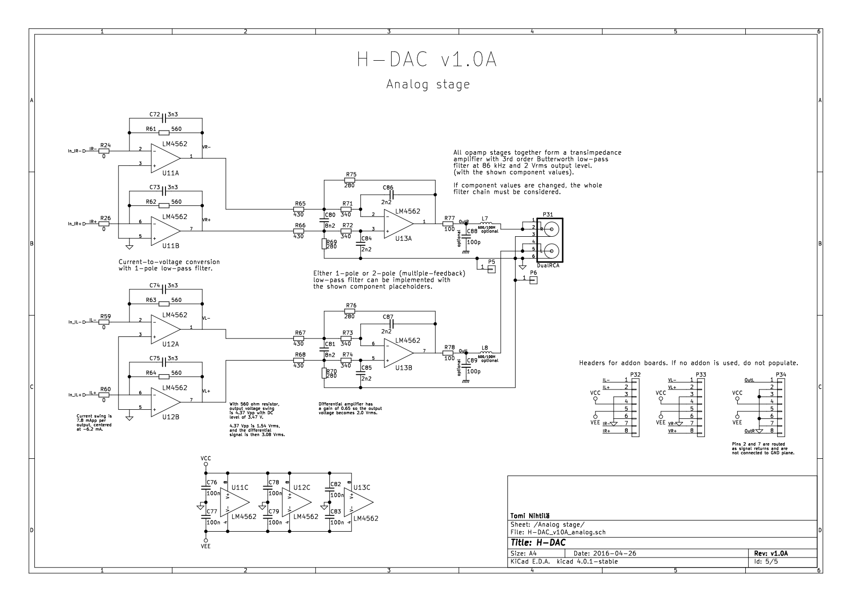
PCM1794A is TI’s flagship delta-sigma DAC accepting 192 kHz / 24-bit signal with differential current output. It is a hardware-controlled version of PCM1792A. Some DAC settings are fixed with external pin connections, while digital filter slope and de-emphasis filter can be changed externally with jumper links in P21. Output is differential current type at relatively high output level of 7.8 mA p-p with common mode level of -6.2 mA. As the output is current, contains some high frequency components, and has large DC-level, some analog circuitry is required.
S/PDIF receiver and DAC schematics
Analog stage
All four current outputs are fed to current-to-voltage (I/V) converters (transimpedance amplifiers) with first order low-pass filters. After this the signal is voltage but still has high DC-level. The differential operation amplifier (U13) circuit with 2-pole multiple-feedback low-pass filter removes the DC-offset, adjusts the output level, and converts the differential signal into ground-referenced single-ended signal. Together the low-pass filters at the I/V-stage and differential stage form a third-order Butterworth low-pass filter at 86 kHz, providing output level of 2 Vrms. This is of course with the shown component values and anyone is free to change these. See section Analog filter design and simulation results for more information regarding the filter design.
Resistor values are very low for good noise performance. L7, L8, C88, and C89 are optional filter components at the output. L7 and L8 can be replaced by 0-ohm resistors as has been done in the prototype.
LM4562 opamps are used throughout the analog stage but almost any good opamp can be a viable option. For example, the oldie and disrespected NE5532 is still an excellent and affordable choice. See my post regarding comparison of LM4562, NE5532, and OPA2134.
Note that schematics show some net names within the analog path – these points are connected to pinheaders P32, P33, and P34. These are used to connect external addon boards to H-DAC. When writing this, the boards available are Addon BalOut, Addon H-PreAmp, Addon H-Filter, and Addon H-MCU. One could design boards for example to experiment with discrete output stages. These pinheaders are in 2.54 mm pitch so even using a veroboard is possible.
Note that there is no output mute circuit. When output opamps are powered up, they are likely to generate possibly loud pop. Therefore, power up power amplifier or active speakers after DAC/preamplifier which is always a good practice to follow.
Analog stage schematics
Control
H-DAC is completely hardware-controlled by jumper links in P21. Available settings are
- Input selector between 5 inputs: coaxial 1/2, Toslink 1/2, and external I2S or USB
- DAC filter slope; see this post for more information
- Closed: sharp filter response (default, kind of…)
- Open: slow filter response
- De-emphasis filter; this is used in some old CDs – otherwise should be disabled
- Closed: disable (default)
- Open: enable
- S/PDIF receiver phase detector rate; I did not see difference in audio measurements
- Closed: high rate; lower in-band jitter but 192 kHz sample rate may not work
- Open: normal rate; higher in-band jitter but sample rates up to 192 kHz will work (default)
U8 translates jumper link positions to appropriate selector signals for CS8416. Instead of using jumper links, mechanical switches can be connected to pinheader P21. For example, toggle switches for filter settings and rotary switch for input selector. See HP Pre 2016 for example implementation.
Reset circuit
Reset circuit description is a bit more complicated as it does have some bugs. The purpose of it is to set DAC into reset state when no signal is played.
The idea is that if there is no S/PDIF signal coming to CS8416 or no input jumper set, one of the signals NV/ERR, ~AUDIO, or NOSEL is high and triggers mute via diodes D8, D9, or D10, which then puts DAC into reset state. Furthermore, D4, R57, and C64 delay reset after powering up the device and similar circuit can be found in CS8416. I have used similar circuit in another design and it works fine. Except I forgot to re-design it after adding the external I2S path! Therefore, if the reset circuit is used as shown, USB and external I2S input do not work as selecting that input would put DAC into reset state.
Why is the reset circuit needed then? Because CS8416 in hardware mode has an annoying feature that it holds the last sample after it loses signal and lock. This means that if input is switched to unlocked input or cable unplugged while playing music, there is a DC-level at the output. Depending on the sample that is held, this level can be very high. And this behaviour can only be changed in software mode. Also PCM1794A’s ‘zero flag’ does not work as input is not zero but constant.
My suggestions in various user scenarios:
- USB/I2S input is not used
- Populate reset circuit as it was intended – it works as designed
- Cx2, Opt2, and USB/I2S inputs are used (as in HP Pre 2016)
- Populate reset circuit with the mod shown in the schematics and below, and it works as designed
- Cx1 or Opt1, and USB/I2S inputs are used
- Do not populate reset circuit, it will not work. You have to live with the potential risk of DC at the output. However, it may not be a real risk because:
- DC-level appears at the output only if you unplug cable while playing or switch to input that is not connected to anything
- This level is almost random – most likely it will not be huge
- In almost all cases your power amplifier or active speakers have high-pass filter at the input which removes the DC; check it before using this option
- Do not populate reset circuit, it will not work. You have to live with the potential risk of DC at the output. However, it may not be a real risk because:
Reset circuit mod is shown below (see schematics). The trace between D5 cathode and R28 is cut, and D5 cathode routed to the top side, pin 9 of U8. This forces CS8416 into reset state with all other inputs except Cx2 and Opt2.
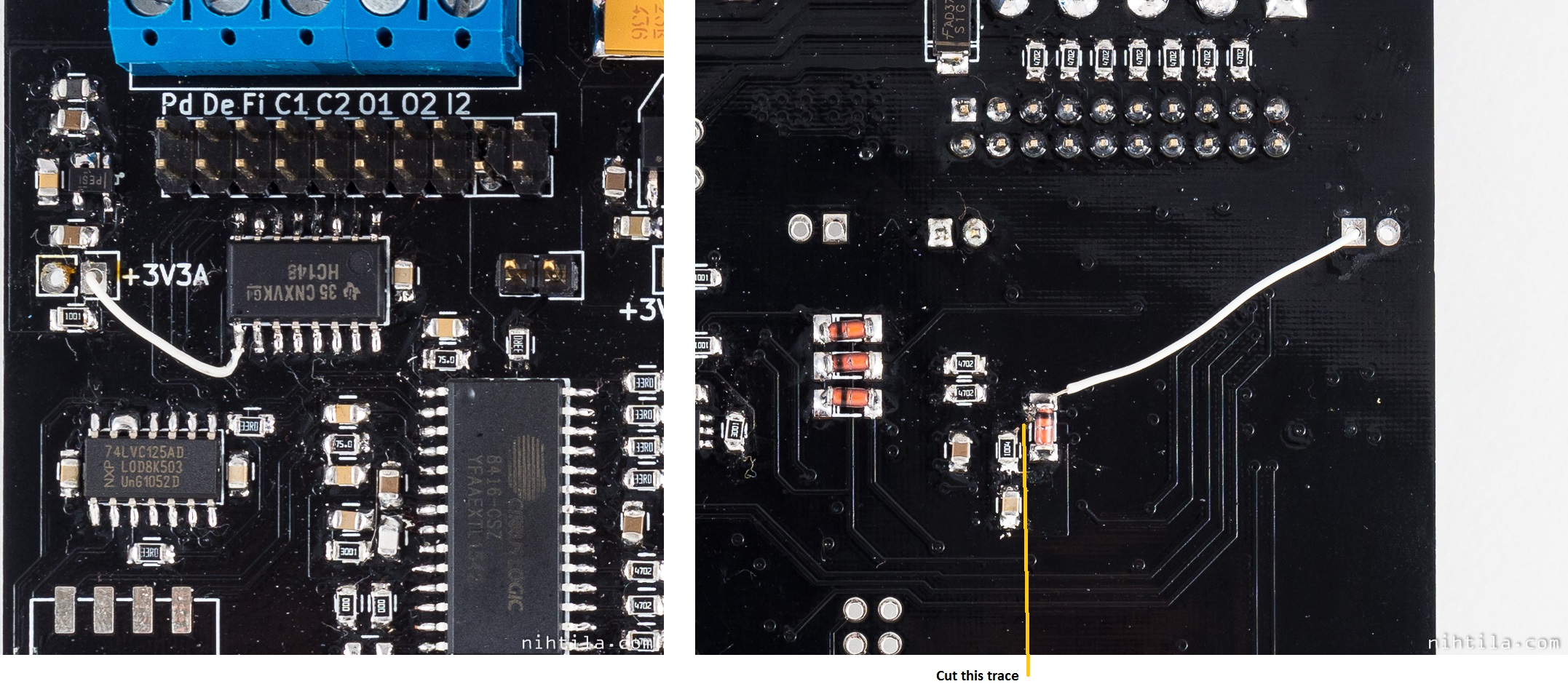
Reset circuit modification
Components
The design relies mostly on 0805-sized SMD components. All components are ‘basic’ ones, nothing exotic. Resistors are thin film type, filter capacitors film, and all other small capacitors ceramic.
Pictured is also the type of USB cable that can be used in place of the on-board USB connector.
Note that in the photographed prototype unit single-ended output stage is not populated as it is being used with a H-PreAmp addon.
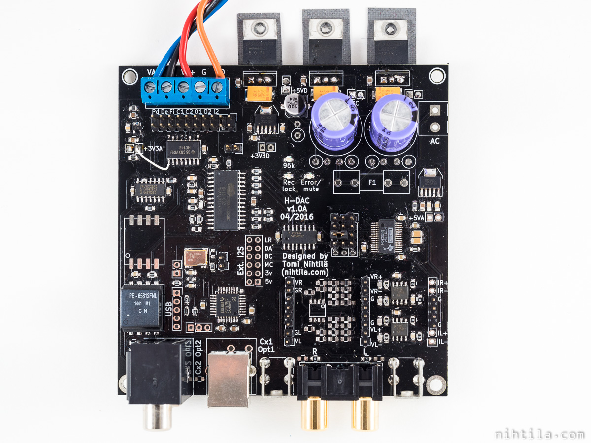
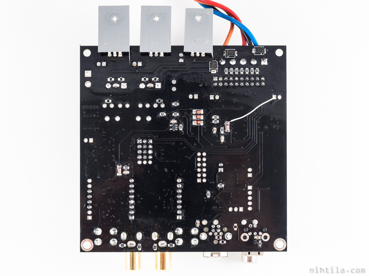

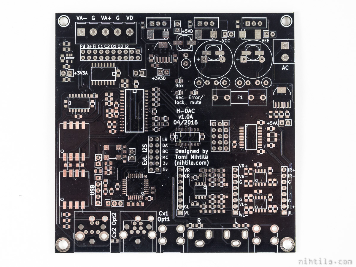
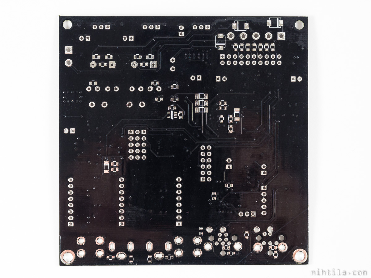
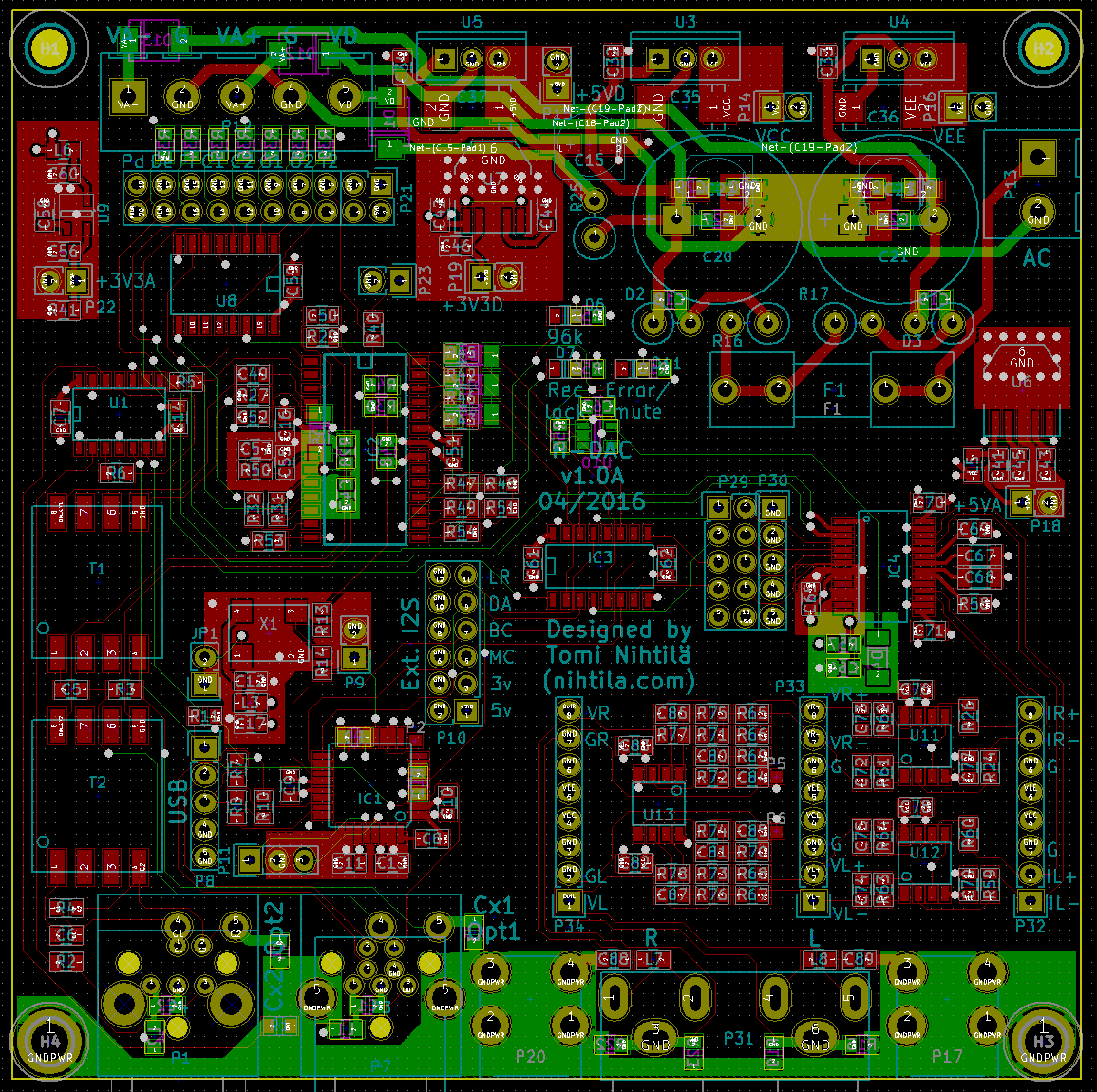
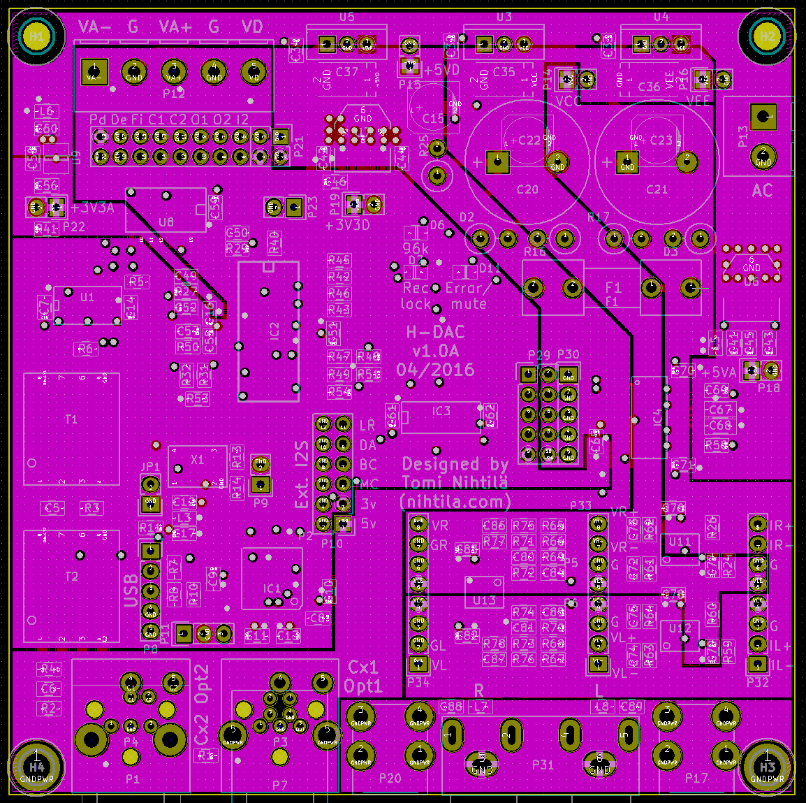
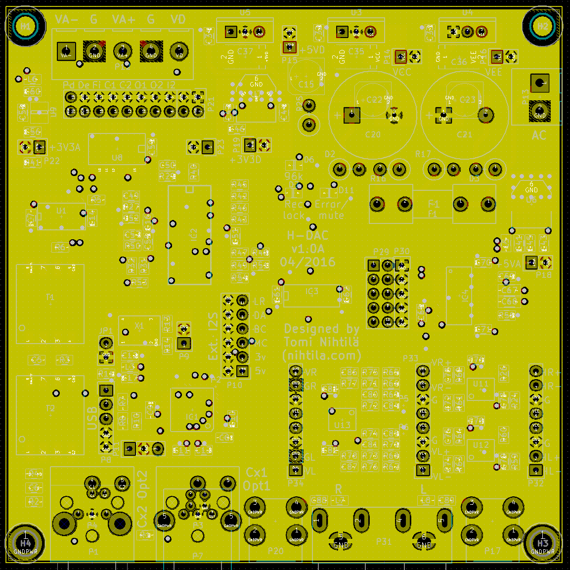
Layout
PCB is 4-layer board with the following stackup: signals, ground, split power, and signals. Layout design is not described here as it is its own complicated matter. I have done my best to make as good layout as possible with the resources and knowledge I have. Measurement results and usability tell how well I have performed. In fact, this is my first “real” 4-layer design and based on the audio measurements I can be quite pleased with it.
Below are layout images
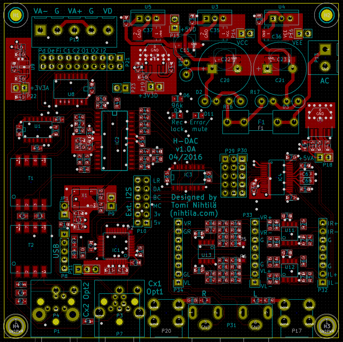
Top layer
Top and bottom layers
Split power plane (above bottom layer)
Ground plane (below top layer)
Analog filter design and simulation results
I used TI’s Opamps for Everyone, chapter 16: Active filter design techniques as a reference for this as analog design is not my strongest point.
I decided to use third order low-pass filter here but lower orders can be used with the same component placeholders if wished. Just leave extra components out and/or replace some with 0-ohm resistors. I chose maximally flat Butterworth filter type. Higher than second order active filters consist of cascaded first and second order stages placed in the order of rising Q-value. This filter has the first stage in the I/V-stage, followed by a second order multiple feedback (MFB) stage.
In Opamps for Everyone, Table 16-5 on page 16-57 presents Butterworth coefficients for 1-10 order filters, and page 16-18 shows formulas for MFB low-pass filter. The corner frequency of the first order filter at I/V-stage follows the normal 1/(2*pi*R*C) formula but the second order MFB-filter has rather complicated formulas for calculating component values. I have created an Excel spreadsheet for calculating the components, screenshot shown below. Shown are the values for H-DAC: gain is 0.65, fc is 86 kHz, C1 is 2.2 nF, and C2 is 16.4 nF. For fully differential amplifier as in H-DAC the schematics can be mirrored. However, the value of C2 will be half of what is shown if only one capacitor is used – 8.2 nF in H-DAC. This gives (approximately) resistor values 430 ohm, 280 ohm, and 340 ohm.
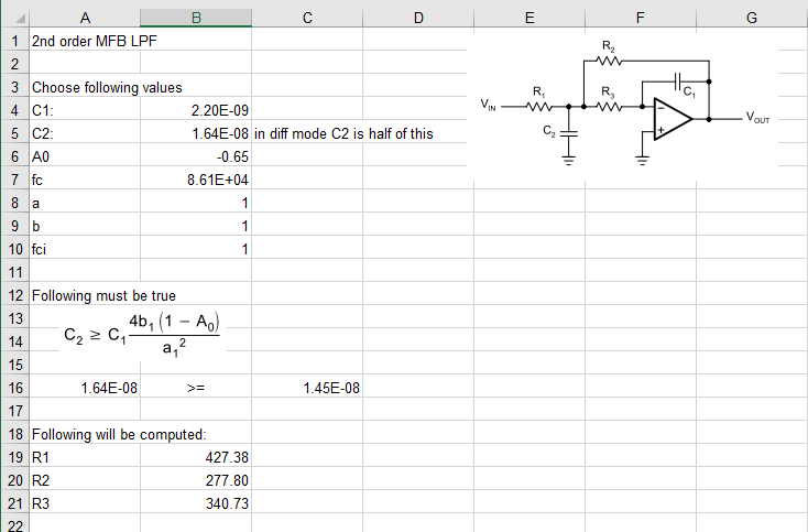
Spreadsheet for filter component calculations
After calculating the component values, it is good to simulate the filter to ensure the response is as intended. Below is a screenshot of the output filter simulation, LTspice files can be found at the end of this page.
Cursor 1 is at 1 kHz, showing 9 dBV amplitude (1.41*2.0 Vrms). Cursor 2 shows -3 dB point at 86 kHz.
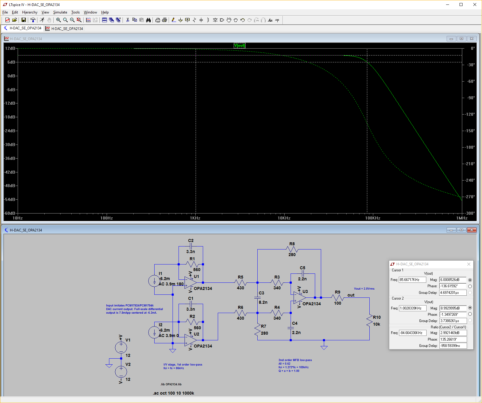
Filter simulation
If you wish to change filter frequency, follow the design procedure described above. If you only need to change the output level, it can be done by changing I/V-stage resistors (R1 and R2 in the schematics above) and keeping the product RC constant – if you halve the resistor value, double the capacitor value.
Measurements
Audio measurements were performed with Audio Precision APx585.
In plot legends, SE refers to single-ended H-DAC outputs (RCA) and BalOut refers to using Addon BalOut.
Measurement conditions:
- Powered by lab supply: 6 V, +14 V/-14 V
- Measurements with Cx2 S/PDIF input
- Simple Toslink and USB measurements provided to verify performance
- Measurement bandwidth is limited to 20 kHz by AES-17 filter
- Analog stage is as seen in the schematics
Key figures
- SNR: 122 dB (A-weighted), 119 dB (non-weighted)
- Noise: -116 dBV (A-weighted), -113 dBV (non-weighted)
- Signal level: 6 dBV (2.0 Vrms)
- THD+N ratio at 2 Vrms / 1 kHz output signal (left/right channel):
- 44.1 kHz: -107/-104 dB
- 48 kHz: -107/-103 dB
- 96 kHz: -103/-98 dB
- 192 kHz: -98/-93 dB
- Crosstalk: -128 dB at 1 kHz, -112 dB at 10 kHz
- USB performance (48 kHz / 16-bit):
- SNR: 99 dB (non-weighted)
- THD+N ratio: -98 dB
- Current consumption: 6 V / +14 V / -14 V
- One Toslink and USB-circuit populated (USB not connected except when in use)
- No BalOut
- Idle, no signal connected: 22 mA / 83 mA / 63 mA
- Idle, S/PDIF-signal connected and locked: 39 mA / 83 mA / 63 mA
- 48 kHz: 40 mA / 85 mA / 65 mA
- 96 kHz: 58 mA / 85 mA / 65 mA
- 192 kHz: 95 mA / 85 mA / 65 mA
- BalOut in use
- Idle, no signal connected: 22 mA / 114 mA / 94 mA
- Idle, S/PDIF-signal connected and locked: 39 mA / 114 mA / 94 mA
- 0 dBFS 1 kHz, Toslink:
- 48 kHz: 40 mA / 118 mA / 98 mA
- 96 kHz: 58 mA / 118 mA / 98 mA
- 192 kHz: 95 mA / 118 mA / 98 mA
- 0 dBFS 1 kHz, USB
- 48 kHz): 58 mA / 118 mA / 98 mA
- No BalOut
- One Toslink and USB-circuit populated (USB not connected except when in use)
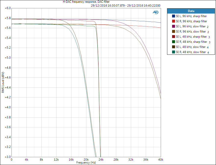
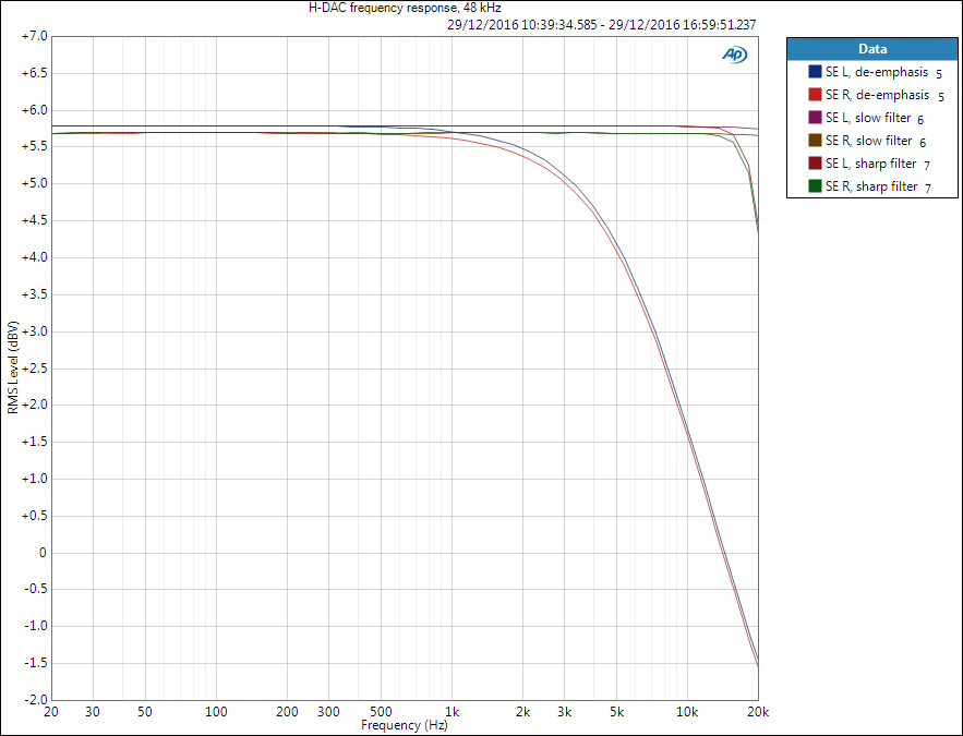
Frequency response
Frequency response of H-DAC at 48 kHz and 96 kHz sample rates are shown below. PCM1794A has two DAC filter settings: sharp and slow. Sharp setting has steep roll-off before Nyquist frequency but remains flat until that, while slow setting have gentle roll-off starting earlier. I have written a post regarding these filters.
There is approximately 0.1 dB difference between channels which is higher than I expected. I think it is a combination of resistor tolerances (which are 0.5 % though) and PCM1794A channel differences. I need to find the root cause of that.
Pre-emphasis filter is rather ancient feature used in some old CDs which was then corrected in DAC de-emphasis filter. It follows pre-defined response, somehow similar to RIAA.
Impulse response
Impulse response for each filter type at 48 kHz is shown below.
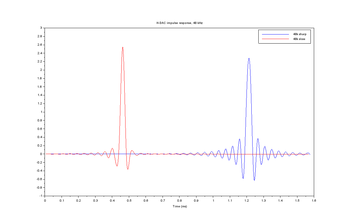
For more information regarding DAC filters and their effect on frequency response and impulse response, see my post regarding the topic.
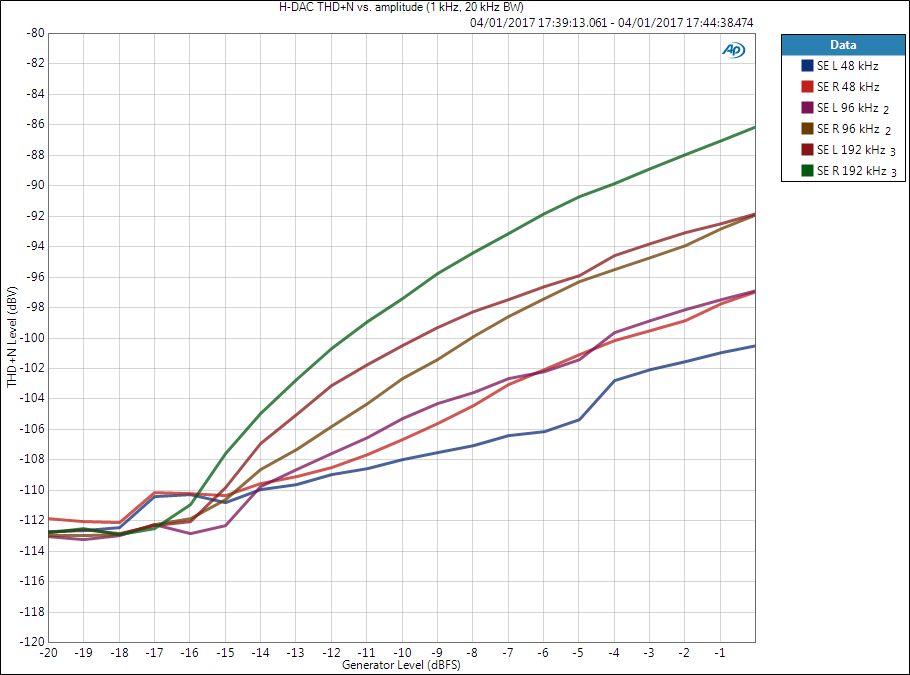
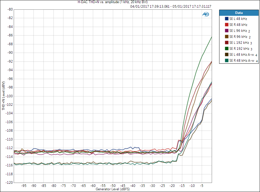
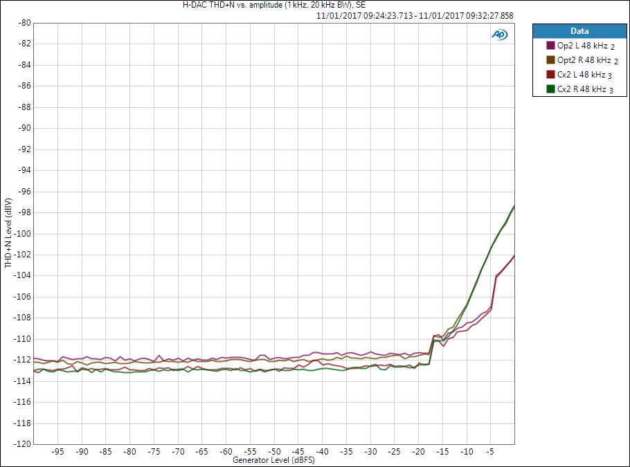
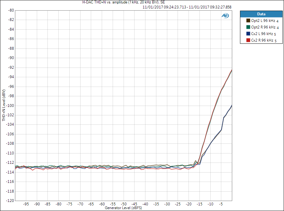
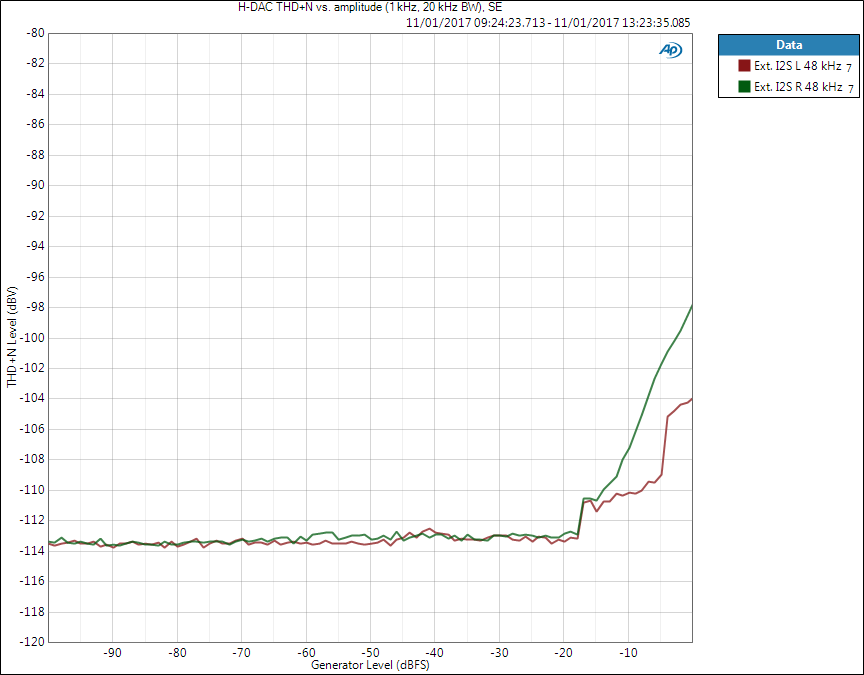
THD+N vs. amplitude
THD+N level in a function of amplitude across sample rates can be seen below. There is no significant difference in noise floor between sample rates (when measurement bandwidth is kept constant). However, distortion increases with higher sample rates, as is also stated in the datasheet. Distortion part zoomed in is shown in another figure.
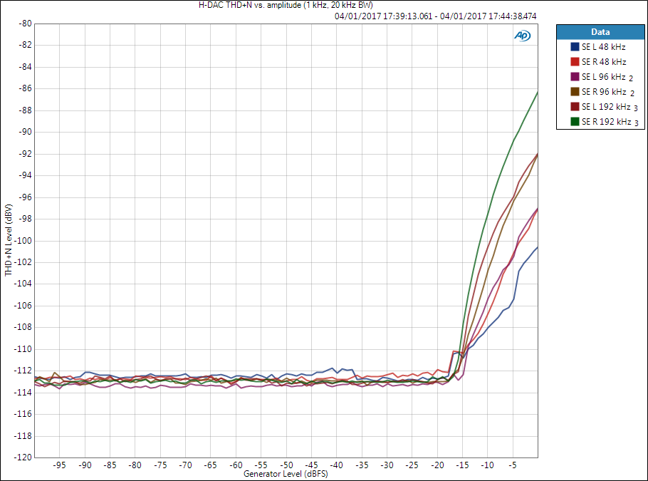
With default component values, H-DAC output level is 2.0 Vrms = 6 dBV. Therefore, SNR or THD+N ratio can be derived by taking the absolute level and adding 6 dB. Below is one trace with A-weighting where noise floor is -116 dB (after rounding). This makes A-weighted SNR 122 dB.
Datasheet gives A-weighted SNR for PCM1794A 123 dB minimum and 127 dB typical for 2 Vrms output – not quite there but very good result anyway. I have not seen significant difference between direct I2S- and S/PDIF-signals.
According to datasheet, typical full level THD+N value also rises 6 dB when doubling sample rate (but measurement bandwidth kept constant). THD+N level at 0 dBFS measured with various sample rates (left/right channel):
- 44.1 kHz: -101/-98 dBV
- 48 kHz: -101/-97 dBV
- 96 kHz: -97/-92 dBV
- 192 kHz: -92/-86 dBV
As THD+N ratio, these numbers become:
- 44.1 kHz: -107/-104 dB
- 48 kHz: -107/-103 dB
- 96 kHz: -103/-98 dB
- 192 kHz: -98/-92 dB
At 48 kHz sample rate, 0 dBFS signal, and 20 kHz measurement bandwidth, the datasheet gives typical THD+N ratio 0.0004 % (108 dB) and maximum 0.0008 % (102 dB). So my measurements are within the limits although the difference between channels remains quite high. I have seen similar gap between channels also with different opamps and even with another PCB. Therefore, if any reader has been measuring PCM1794A (or PCM1792A) I would be keen to hear your measurement results, especially regarding the channel differences.
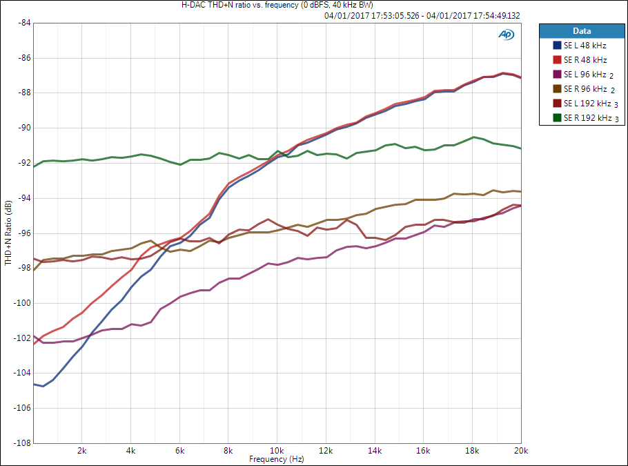
THD+N ratio vs. frequency
This is measured as ratio, not level. Note also that measurement bandwidth is doubled to 40 kHz to get more harmonics in. Differences between channels seem to get smaller with higher frequencies and are by far the largest with 192 kHz sample rate. The reason for these differences is still unknown.
Crosstalk
Crosstalk is shown in level with 0 dBV output signal amplitude. Slight peaking around 10 kHz can be seen with single-ended output but with BalOut it is absent.
Input comparison: coaxial, optical, USB, and external I2S
All measurements above were performed with Cx2 coaxial S/PDIF input. Below are THD+N vs. amplitude measurements for Cx2 and Opt2 inputs, with 48 kHz and 96 kHz sample rates. At 48 kHz noise floor is 1 dB higher with Toslink input. It is worth reminding that source in these measurements is extremely high quality measurement instrument.
External I2S is measured below. This is just direct I2S to the DAC chip, thus in practice the quality of I2S clocks will affect performance.
USB playback
USB is very different case. It is implemented with TI PCM2707C which is capable of “only” 16-bit 48 kHz signal. Also, it recovers I2S clocks from USB with its own PLL and external 12 MHz oscillator.
First of all, when USB is connected but no signal is played back, noise level increases from -113 dBV to -107 dBV. As DAC is idling and data signal is all zeros, this must be due to poorer clock signals or noise coupling from the PC. Anyway, nothing alarming here.
When signal is played back, noise floor increases to -93 dBV. This must be just due to 16-bit data – dynamic range is fundamentally limited by the digital signal.
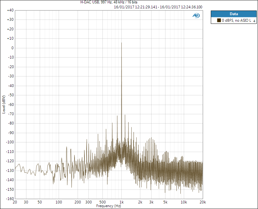
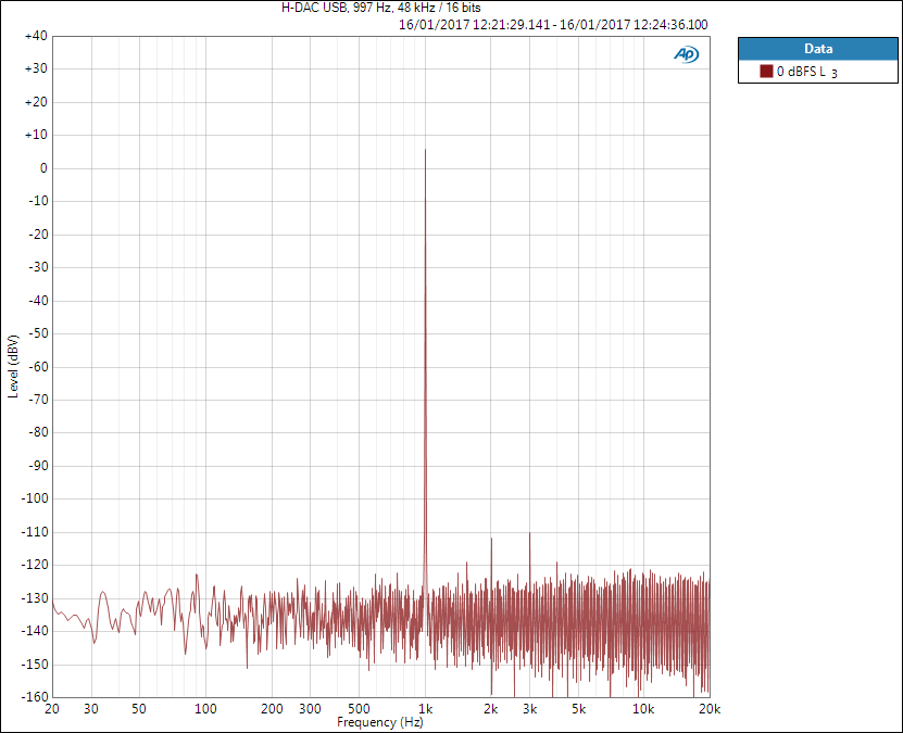
The biggest issue in USB playback can be the PC, namely, Windows. I have written another post regarding USB playback and getting good quality signal out. The issue relies in operating system level resampling and whatever they do. Therefore, you probably want to get bit-perfect playback. As an example, below I have played 997 Hz tone with foobar2000 with and without ASIO4All drivers. The difference in THD+N level is whopping 15 dB. Just because Windows is doing “something” we have no direct control over.
See other USB performance figures in Key figures list above.
Measurements with AC supply
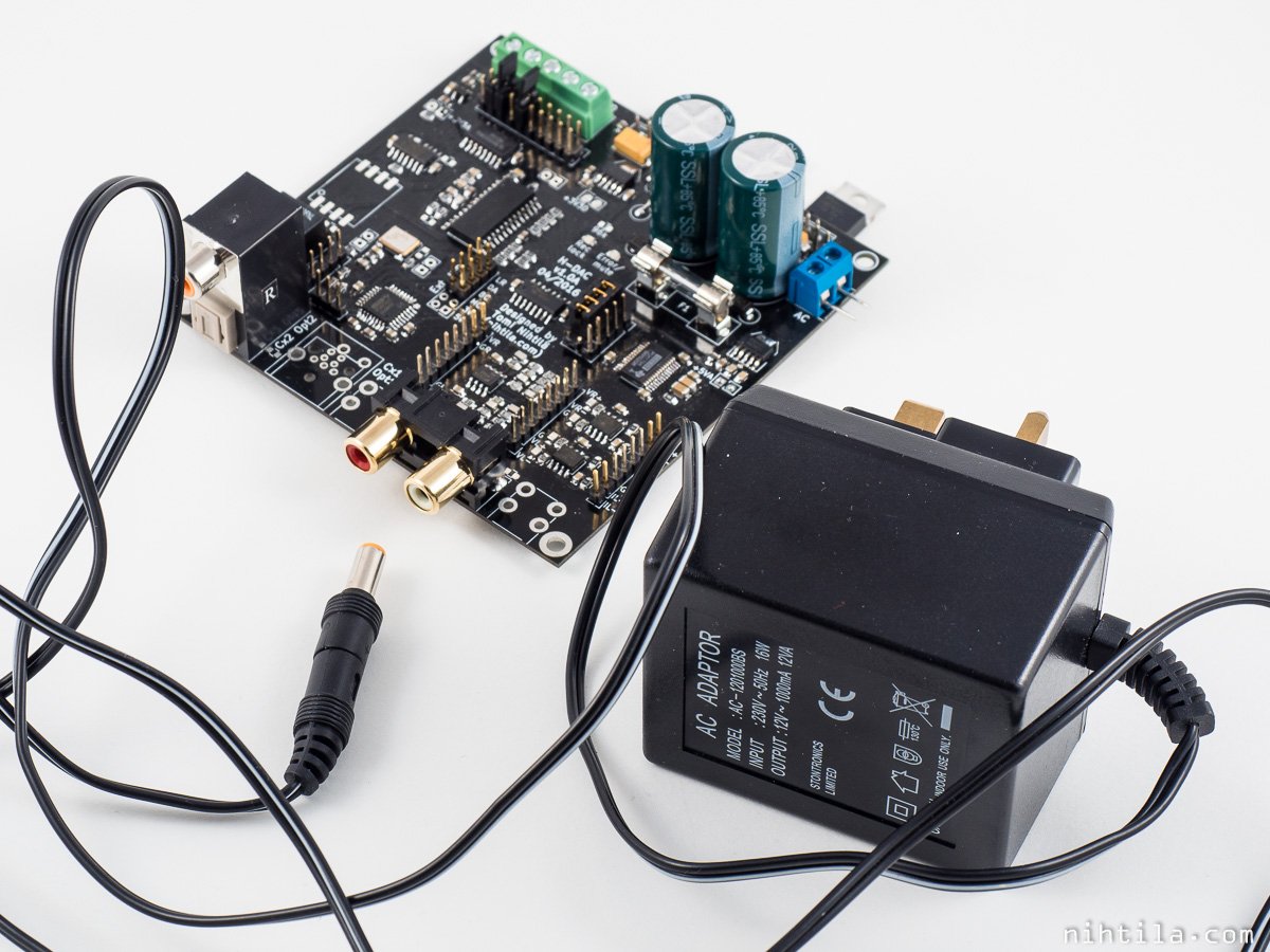
I did not run extensive measurements but quickly checked that there was no major issues. Some measurements maybe showed slightly lower results (1-3 dB) but nothing major. Therefore, AC supply is also a viable option. I used 12 VAC 1 A wall supply shown below.
Sound quality
This is certainly very interesting feature of an audio product. However, it is also very subjective and personal matter. I also do not have enough references to compare H-DAC to some other DACs. I will try to add some notes later when I have few products to compare with. I will also do some experiments with various output stages at later time.
I could possibly say that a DAC like H-DAC aims to be very transparent component in the signal chain. It has technically very high performance – very low noise, very low distortion, minimal out-of-band signal energy; it should not add or remove anything from the signal. High fidelity for the original signal, if I may say. This leaves the stage for the components that colour the sound more: power amplifier and speakers/headphones.
Files
- v1.0A files
- Schematics
- Component placement top
- Component placement bottom
- BOM
- Check carefully before making component order
- Prices are in GBP, without VAT, and not up-to-date)
- LTSpice simulation
References and additional information
- LM4562 datasheet
- CS8416 datasheet
- PCM1794A datasheet
- PCM1794A output stage opamp measurements: LM4562, NE5532, and OPA2134
- Bit-perfect ASIO drivers to solve issues with Windows audio quality
Version history
Schematics / PCB version history and known errors and bugs
- v1.0A Initial version
- Re-design reset circuit (see details in Reset circuit section above)
- Consider replacing the RCA/Toslink combo connector for future revisions due to its rather poor mechanical design
- What is causing the differences between channels in THD at full output level?
- Remove 96KHZ led as it is not working as understood
- Use thermals everywhere for easier soldering
This page version history
- 15.1.2017 Initial version
6 comments
Where can I get one?
This was never really on sale except bare PCBs. It was more like my learning platform and was not very cost effective. But the performance is great and one is in my constant use. I think I do have 2-3 almost fully assembled ones I could sell. I will send you an email.
Hi! I find it interesting that you used the PCM2707 for the I2S signal. Is there any reason for not using another more “capable” IC?
PS: I just found out your website and let me tell you that it’s amazing! I’ve been looking at stuff you have done and it’s pretty much what I want to make in the future. I’m working right now on the PCM2912A DAC and I’m using your design as a bit of a reference too ahah.
Keep it up!
PCM2707 was used just because it is one of the only easy options to use. Chips capable of more high resolution formats are unfortunately not just a matter of buying a chip and soldering it in place. First of all, they are not as easy to buy, and there are firmware, drivers, and licenses involved. I am not exactly sure what it would take to use eg. XMOS chip. However, the easiest solution for direct USB-I2S in DIY DACs is just to provide external I2S in the DAC and buy a third party USB-I2S module. Maybe one day I will try to figure out how tricky it would be to make my own implementation.
Thanks for the kind words! I have been working on new prototypes now during holidays and will post something new shortly.
Yeah the complexity creep is indeed a thing. I though that it wouldn’t be too hard to make something more capable than a PCM2XXX based DAC but when I actually saw what it takes to build one…well let’s start with the basics ahah
PS: Am I supposed to get a notification from your replies? If so, I didn’t get any :/
I’m not sure about notifications. Quickly checking it seems not to be a feature of Wordpress. But thanks for letting me know, I can look at that later.