
- Very high performance preamplifier; measurement results with H-DAC and 2 Vrms output:
- Dynamic range / SNR: 116 dB (A-weighted)
- THD+N ratio: -102 dB (2.0 Vrms / 1 kHz, 48 kHz sample rate)
- Crosstalk at 10 kHz: -113 dB
- Very high performance headphone amplifier
- Dynamic range / SNR: 115 dB (A-weighted)
- Maximum output power / THD+N ratio:
- 22 mW / -98 dB into 560 ohms
- 230 mW / -85 dB into 33 ohms
- More gain can be added for higher output power
- Software controlled (Arduino compatible)
- Balanced outputs (XLR) on-board and unbalanced connectors (RCA) on H-DAC board
- Takes supplies and audio signals directly from H-DAC via pinheaders
- 10×10 cm 4-layer PCB shaped to fit tall components on H-DAC board; PGA4311 volume control, LM49724 and LM4562 opamps (or any with the same pinouts), TPA6120A2 headphone amplifier, optional THAT1606 balanced drivers
H-PreAmp is an addon board for H-DAC, transforming the fixed-output DAC into a very high quality preamplifier with integrated headphone amplifier. H-DAC and H-PreAmp together provide single-ended (RCA) and balanced (XLR) outputs as well as headphone amplifier.
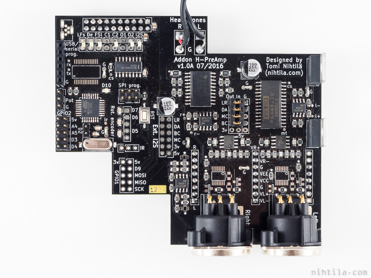
Signal is kept differential all the way from the DAC chip to balanced outputs and headphone amplifier. 4-channel volume control is used to achieve that and as it is SPI-controlled, microcontroller with software is required. Microcontroller block can be made Arduino compatible for easier software development using the Arduino IDE familiar to many. Hardware supports connectivity for potentiometer, rotary encoder, display, infra-red receiver, switches, etc.
Line output level and headphone amplifier gain can be adjusted to meet the requirements by changing resistor values.
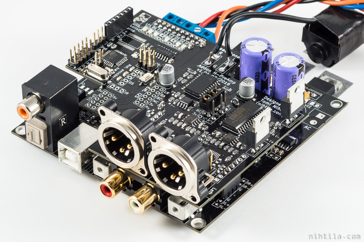
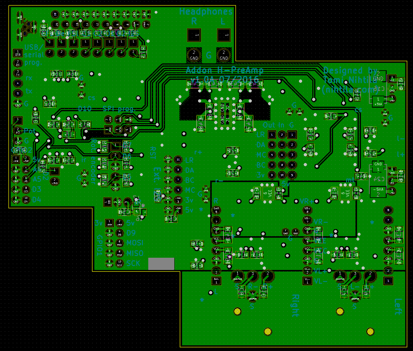
Addon H-PreAmp stacked on H-DAC.
Design and schematics
Addon H-PreAmp is stacked on pinheaders of H-DAC where audio signals are taken from after I/V-stage, and then routed through differential buffer and software-controlled volume control followed by headphone amplifier and output buffers. Balanced XLR-connectors are on-board H-PreAmp and unbalanced signals are routed back to H-DAC using its RCA-connectors.
On-board ATmega328P controls volume as well as input selector and DAC settings via H-DAC jumper link pinheader. The microcontroller circuit is Arduino Nano compatible when pre-loaded with corresponding bootloader.
Board shape is due to tall components on H-DAC.
Note that some component values have changed after taking photos – this is not the final version in use.
Addon H-PreAmp consists of input stage, volume control, and three parallel output stages: balanced output, unbalanced output, and headphone amplifier. Microcontroller circuit takes care of control signals.

Root schematics (block diagram)
Power supply
H-PreAmp uses pinheaders P1, P2, and P5 (single-ended output -sheet) for audio signals and also gets +12/-12 supplies for opamps. Digital supplies are routed via H-DAC’s jumper link -pinheader P18 (microcontroller -sheet). Therefore, the only regulators required on H-PreAmp are 5-volt versions of LM2940/2990 for PGA4311. Plenty of local decoupling capacitors are used as well.
Input and volume control
Audio comes on board via P1. This is the differential voltage signal after I/V-stage on H-DAC and still contains common-mode voltage which is removed by fully differential buffers U3 and U5. Buffer stage also includes second order low-pass filter similar to the H-DAC board – providing total 3rd order Butterworth filter together with the I/V-stage filter. 4-channel SPI-controlled volume control PGA4311 is used to adjust the signal level. As its output driving capabilities are not superb, buffers U7 and U8 have been added. These are in inverted configuration for possibility to add gain or attenuation – this gain affects all outputs. Note that the signs in signal labels are swapped due to inverting stages. 10-ohm resistors offer some isolation before dividing the signal for balanced outputs, unbalanced buffer, and headphone amplifier.
Do not change component values on differential buffer without considering the whole 3rd order filter formed by the I/V-stage and this buffer state. See H-DAC page for more information.
Fully differential buffers U3 and U4 have Vcom (output common mode signal) and EN (enable) pins connected to ground via 0-ohm resistors. These are correct connections for the shown LME49724 opamp but may differ in some other models; for example, for some opamps it is recommended not to connect Vcom to ground directly.
Measurement results are provided for the shown opamps but feel free to use any preferred model with the same pinouts.

Input and volume control schematics
Balanced output
Balanced output section contains a possibility to place THAT1606 balanced drivers for transformer-like output for very high common mode rejection in balanced interconnects. Unfortunately, as has been shown in Addon BalOut page, noise-wise these ICs are behind the best ICs such as the ones used in the H-PreAmp. These are recommended only if very high CMRR is really needed. For the best performance, omit U1, U2, and their external components, and bypass these buffers with resistors R1-R4. From CMRR point of view this will not provide as good balance (determined by series resistors R7-R10 and bypass resistors R1-R4) but significant improvement in noise floor. I have included placeholders for various filtering and protection components shown in THAT1606 datasheet, and these are optional and not used in the prototype. Short L1 and L2 with 0-ohm resistors if ferrites are not used. To be honest, I think these should be on the connector side of the capacitors although they are shown like that in the datasheet.
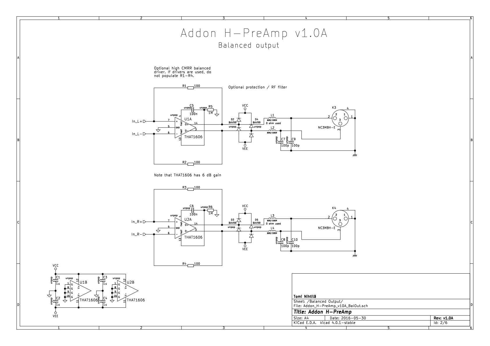
Balanced output schematics
Single-ended output
This simply adds up the positive and negative legs of differential signal. Output is routed back to the H-DAC board’s RCA connectors. R50 and R51 provide alternative ground path as ground trace is taken to H-DAC via P5 making it quite long. These are not needed in normal operation.
Gain of single-ended output relative to balanced and headphone outputs can be adjusted with these resistors.

Single-ended output schematics
Headphone amplifier
Headphone amplifier is TPA6120A2 circuit from the datasheet which is a simple differential amplifier. Note that TPA6120A2 amplifier halves marked L/R are swapped for better routing. Adequate supply bypassing and energy reservoir is provided.
Headphone amplifier gain relative to single-ended and balanced outputs can be adjusted with these resistors. In the example, a gain of a bit less than 2 is added. This may be necessary with high-impedance headphones.

Headphone amplifier schematics
Notes regarding signal level
As filter components around differential buffers U3 and U5 are chosen to be the same as in H-DAC for simplicity, signal level at 0 dB gain is 2 Vrms after the PGA4311. By default there is no gain added in the buffers U7 and U8. As balanced output is taken directly from that stage (when THAT1606 is not used), this is also the balanced output level. By default, single-ended output is also the same level but can be changed with resistors. Note that if THAT1606 is used, it adds 6 dB gain on the balanced outputs.
With the shown component values, headphone amplifier TPA6120A2 has a gain of a bit less than 2 (1000/560), making the total output level approximately 3.6 Vrms, or 11 dBV. When driving low impedance headphones, the effective level drops due to the 10-ohm series resistor which is required for stability. Refer to TPA6120A2 datasheet also if changing the gain resistors as stability may become an issue under some circumstances.
Microcontroller circuit
All control is handled by ATmega328P microcontroller which can be made Arduino compatible with FT232RL USB-serial IC and mini-USB connector, or with an external USB-serial converter on P14. See the related post for more information regarding Arduino compatibility. Some ideas for possible hardware connectivity options:
- Normal potentiometer on P12 connected to microcontroller ADC (used in HP Pre 2016)
- When used in conjunction with R70 and internal pull-up resistor, software can detect when potentiometer is connected. In normal operation the ADC input never goes to VCC – but it does so when the pot is disconnected.
- Infra-red receiver on P11
- Choose suitable supply voltage by populating L6 OR L7, not both
- Rotary encoder on P13
- For volume control, menus, etc.
- Extra leds D1 and D8
- SPI on P8 or I2C on P9
- E.g. for displays
U12 shift register allows microcontroller to control the jumper-pinheader on H-DAC with minimal use of I/O ports. This can also be left out and still use jumpers. Placeholders for LEDs are for automatic display of chosen input and settings. These placeholders have through-hole footprints if one wants to connect the LEDs to front panel.
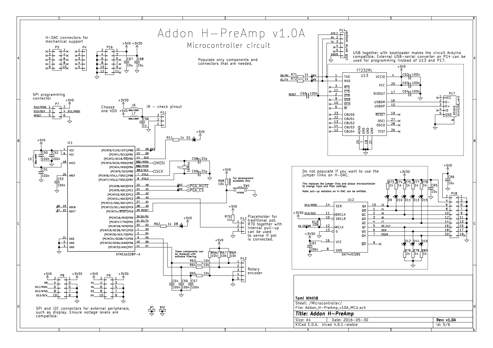
Microcontroller circuit schematics
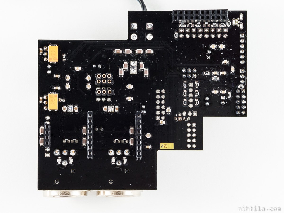
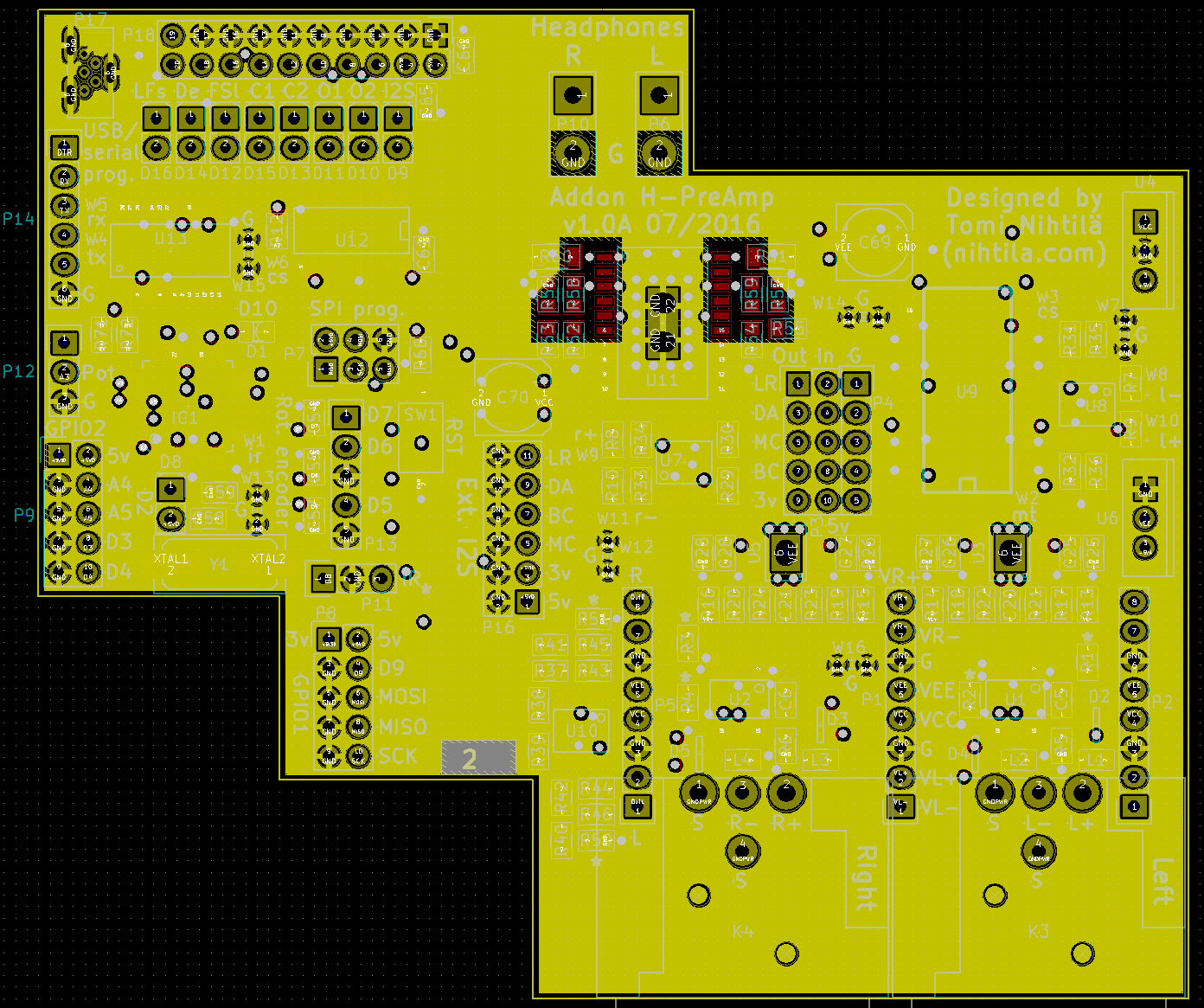
Components and layout
The design relies mostly on 0805-sized SMD components. All components are ‘basic’ ones, nothing exotic. Resistors are thin film type, filter capacitors film, and all other small capacitors ceramic.
PCB is 4-layer with the following stackup: signals, ground, split power, signals. Layout design is not described here as it is its own complicated matter. I have done my best to make as good layout as possible with the resources and knowledge I have. Based on the audio measurement the result is very good. PCB shape allows using big electrolytic capacitors and input connectors.
Note that MC and BC in I2S clock names between CS8416 and PCM1794A (Out/In) on silkscreen are wrong way.
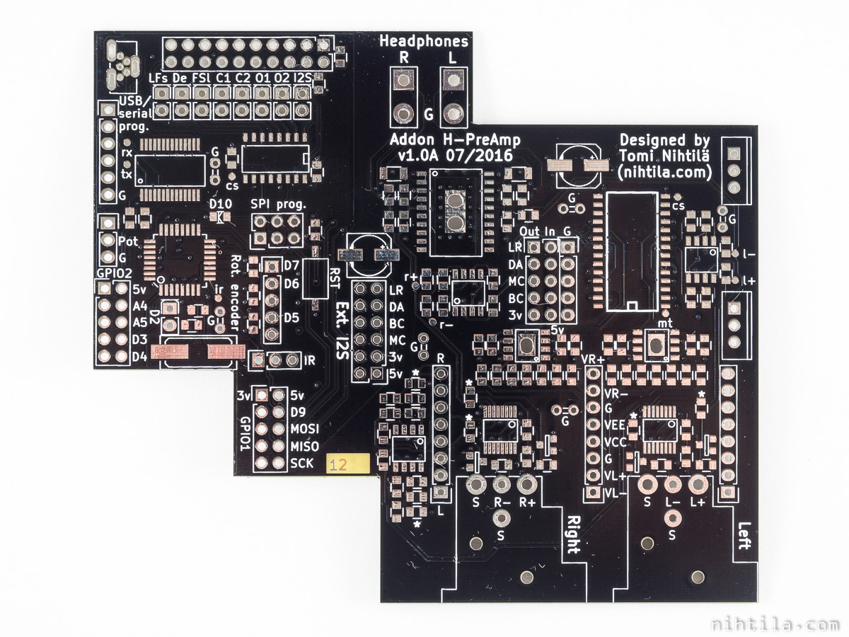

Below are layout images

Top layer
Ground plane (below top layer)
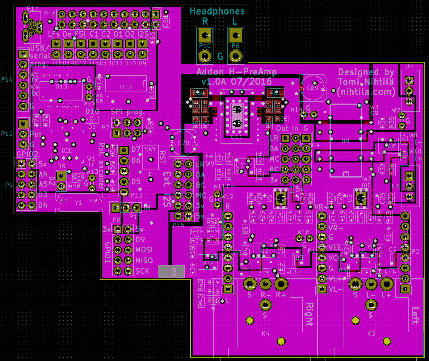
Split power plane (between bottom and ground)
Bottom layer
Software
Although microcontroller circuit is made Arduino compatible, the software I use in my own device is not Arduino sketch but pure C-program developed in Atmel Studio and programmed with AVR Dragon. It is based on code from my old project. The C-file is available here. Note that this is not tested well although it has been working without flaws. This description is for the program used in HP Pre 2016.
Hardware connections are as follows:
- Potentiometer connected on PC3 (AD-converter pin)
- Front panel LED on PD2 (power-on LED)
- Volume indication LED on PB2 (blinks when pot is moved and volume updated)
- PDUR jumper link on PC4
- DAC filter switch on PC5
- Input switch on PD3 and PD4 (this is an on-off-on switch used to select between coax2, opt2, and USB)
All the software do is monitor the potentiometer and switch positions. If something happens, it performs an action to change volume or input/filter/pdur setting. The operation is interrupt-based and functions are as follows:
- Initializations
- Set up ports, pins, and SPI
- Timer0 is set to trigger ADC read approximately 60 times per second
- ADC is set to raise an interrupt when a conversion is complete
- When AD-conversion is complete
- Check that value is within acceptable limits
- Add the new value to the ADC buffer
- Calculate new average value; actual ADC value that is used for volume control is an average of few readings
- Call volume update
- Calculate new average value
- Remove the smallest and largest value in the buffer and calculate average from the rest
- Switch change
- Send new value via SPI to the shift register
- Error occurred (error handling is limited but some illegal values are monitored)
- Mute PGA4311
- Light led
- Eternal loop
- Volume update
- Check if volume has changed from previous value
- If it has, scale ADC reading to 0…MAX_VOL value (scaling has been tuned to give smoothly changing volume when turning the knob – this depends on the used pot type)
- Update PGA4311 via SPI (the same data for all 4 channels)
See the C-file for more detailed explanation.
Measurements
See filter simulation results on H-DAC page.
Audio measurements were performed with Audio Precision APx585. These measurements are done on H-DAC + H-PreAmp combination. Both are fully populated, H-DAC having all regulators, Cx2, Opt2, and USB populated. Stacked device is powered by lab power supply providing +6.2 / +14 / -14 V for VD / VA+ / VA-. Input signal is connected to Cx2 and DAC-filter is set to sharp unless otherwise mentioned. Measurement bandwidth is 20 kHz in noise measurements.
Key figures
- Preamplifier
- Dynamic range / SNR: 116 dB dB (A-weighted)
- Noise level: -110 dBV (A-weighted)
- Maximum signal level: 6 dBV
- THD+N ratio at full output level (left/right channel):
- 48 kHz: -104/-102 dB
- 96 kHz: -99/-98
- 192 kHz: -94/-92
- Crosstalk: -125 dB at 1 kHz, -113 dB at 10 kHz
- Dynamic range / SNR: 116 dB dB (A-weighted)
- Headphone amplifier
- 33 ohm load
- Dynamic range / SNR: 115 dB (A-weighted)
- Noise floor: -106 dBV (A-weighted)
- Maximum signal level: 9 dBV
- THD+N ratio at maximum output (1 kHz): -85 dB / 230 mW
- THD+N ratio at 10 mW (1 kHz): -85 dB
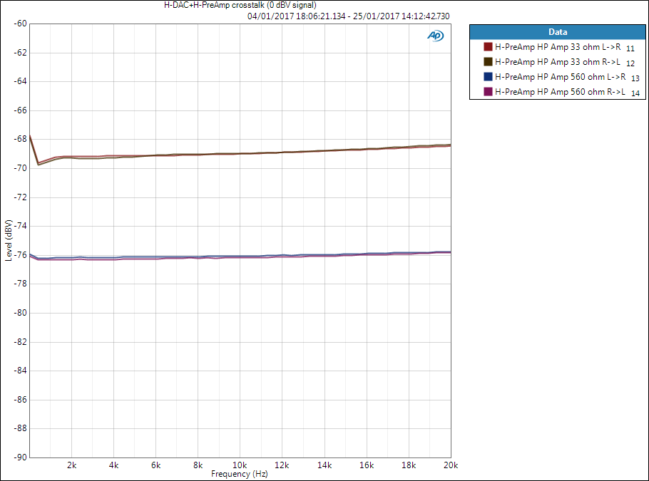
- Crosstalk: -69 dB at 1 kHz, -69 dB at 10 kHz
- Dynamic range / SNR: 115 dB (A-weighted)
- 560 ohm load
- Dynamic range / SNR: 115 dB (A-weighted)
- Noise floor: -104 dBV (A-weighted)
- Maximum signal level: 11 dBV
- THD+N ratio at maximum output (1 kHz): -98 dB / 22 mW
- THD+N ratio at 10 mW (1 kHz): -99 dB
- Crosstalk: -76 dB at 1 kHz, -76 dB at 10 kHz
- Dynamic range / SNR: 115 dB (A-weighted)
- 33 ohm load
- Current consumption (Cx2 input):
- Idle (signal locked): 64 mA / 180 mA / 141 mA
- 48 kHz sample rate, 0 dBFS 1 kHz signal: 64 mA / 190 mA / 151 mA
- Full output from headphone amplifier into 33 ohm: 65 mA / 257 mA / 216 mA
- 192 kHz sample rate, 0 dBFS 1 kHz signal: 124 mA / 195 mA / 151 mA
As can be seen, current consumption from +12/-12 rails is quite high, thus the regulators may become very hot if their voltage drop is high.
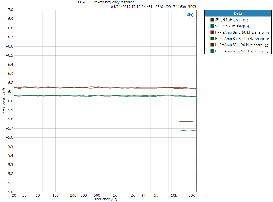
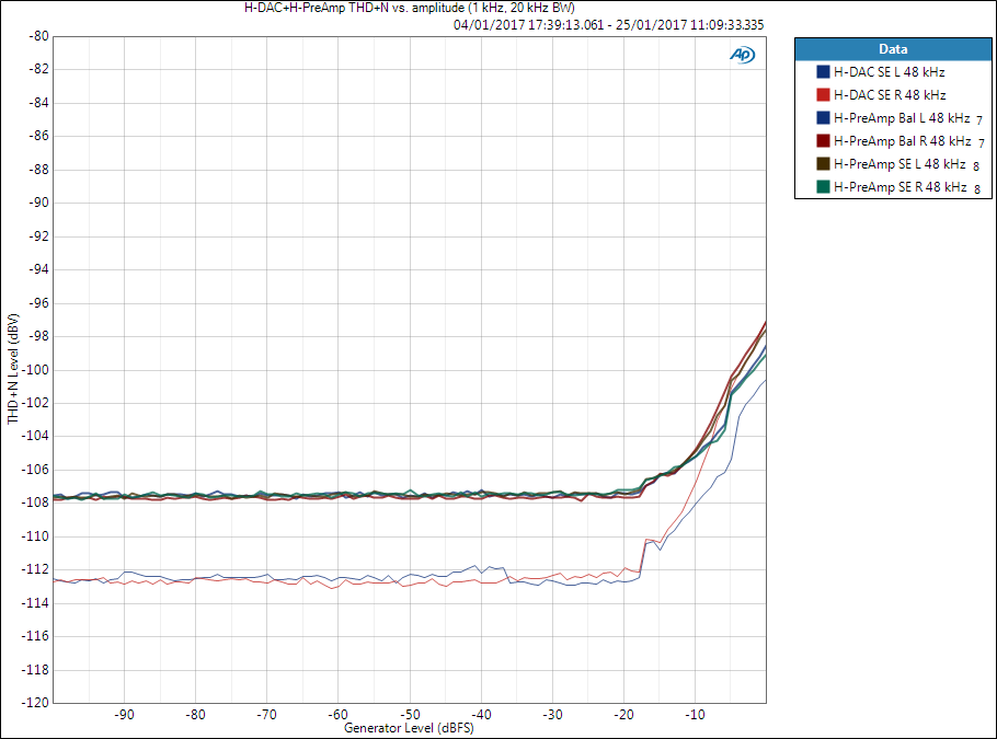
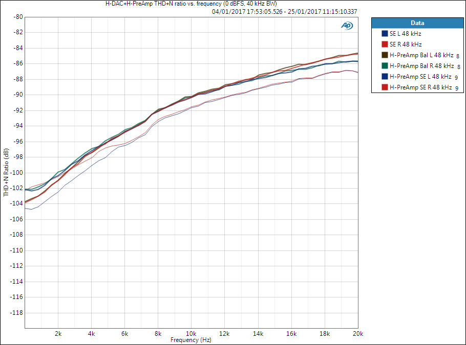
Measurements have been divided into preamplifier and headphone amplifier sections. Many graphs show H-DAC-only measurements for comparison. Volume is set to full 0 dB level.
Preamplifier
Frequency response and output level
No surprises in frequency response. Output level is slightly higher than in H-DAC (thin lines). Small channel difference is still present as it comes somewhere before H-PreAmp.
Noise level and THD+N vs. amplitude
Noise level is 5 dB higher than in H-DAC. I measured noise after LME49724 differential buffer, after PGA4311, and at the output. PGA4311 is the weakest link in this chain and restricts the noise performance. Distortion is similar to the weaker channel of H-DAC.
DespitePGA4311 also does not act like a true analog potentiometer but its behaviour is closer to digital volume control; noise level does not decrease much when turning down volume. I will come back to this topic with separate post one day.
A-weighted noise level is -110 dBV, giving SNR/DR of 116 dB with 6 dBV signal level.
THD+N vs. frequency
Distortion at maximum level follows H-DAC curves (thin lines) but is approximately 2 dB higher.
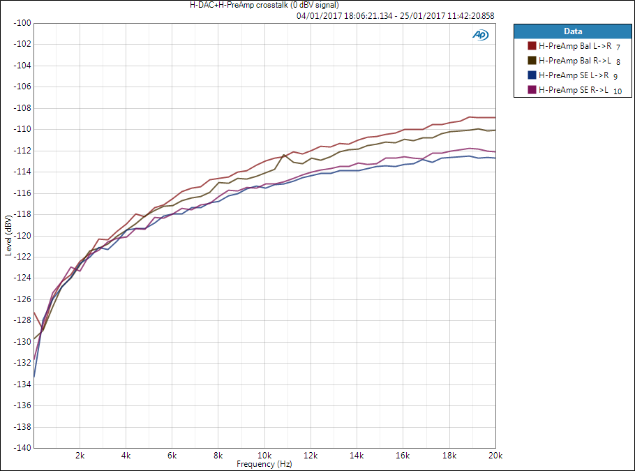
Crosstalk
Crosstalk is good if slightly weaker than in H-DAC only (not shown here).
Headphone amplifier
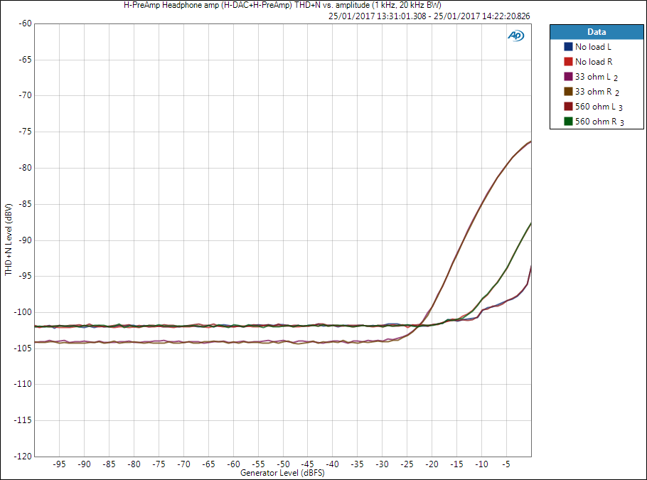
THD+N vs. amplitude
No load and 560 ohm load results are the same. Noise level is -102 dBV and distortion figures differ between channels. Same distortion difference between left and right channel is here as earlier in the signal chain.
Noise level is lower with 33 ohm load but distortion starts earlier – but is consistent across channels.
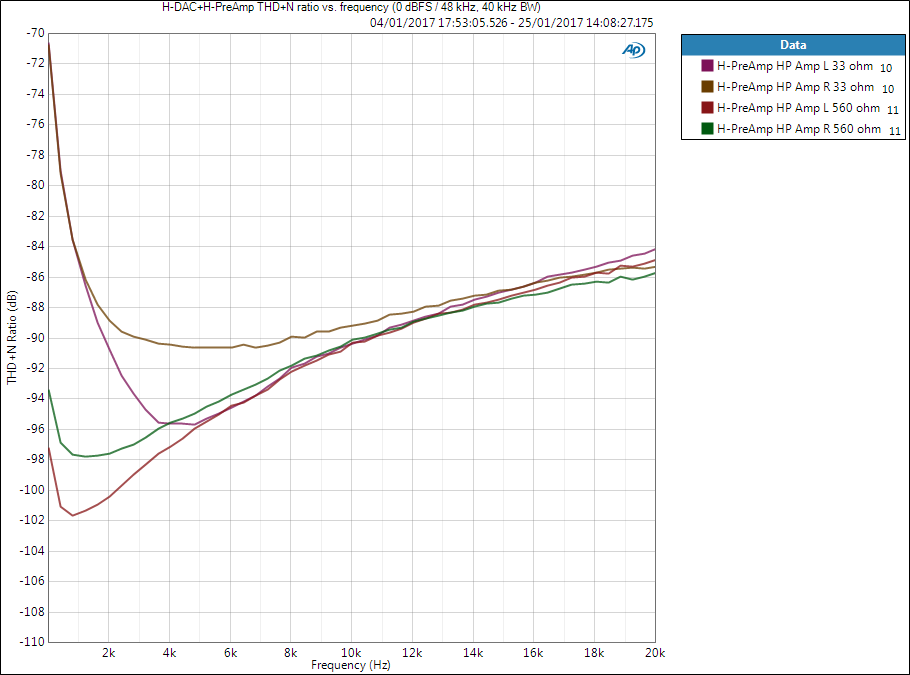
THD+N vs. frequency
This is interesting. I do not know why there is so much more distortion at low frequencies, especially with 33 ohm load. I wonder if there is something limiting the current driving capabilities at low frequencies. There are also significant differences between channels.
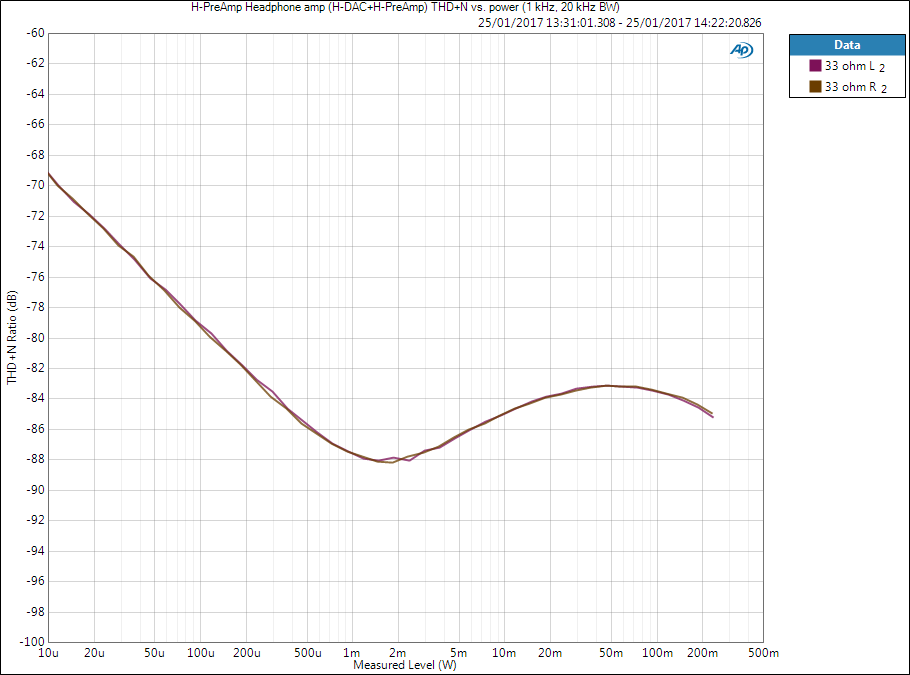
THD+N vs. power
As we are measuring a power amplifier, this is probably the most interesting curve as it shows how much power at what distortion level the amplifier can provide.
Into 560 ohms the maximum output power is a bit over 20 mW. There are differences between channels as was seen in the THD+N vs. amplitude measurement. With this high load impedance the output power is only limited by the voltage swing – current remains small. Therefore, if lots of power is required for high impedance headphones, this can be easily done by adding more gain. Over all the distortion stays very low into high-impedance load.
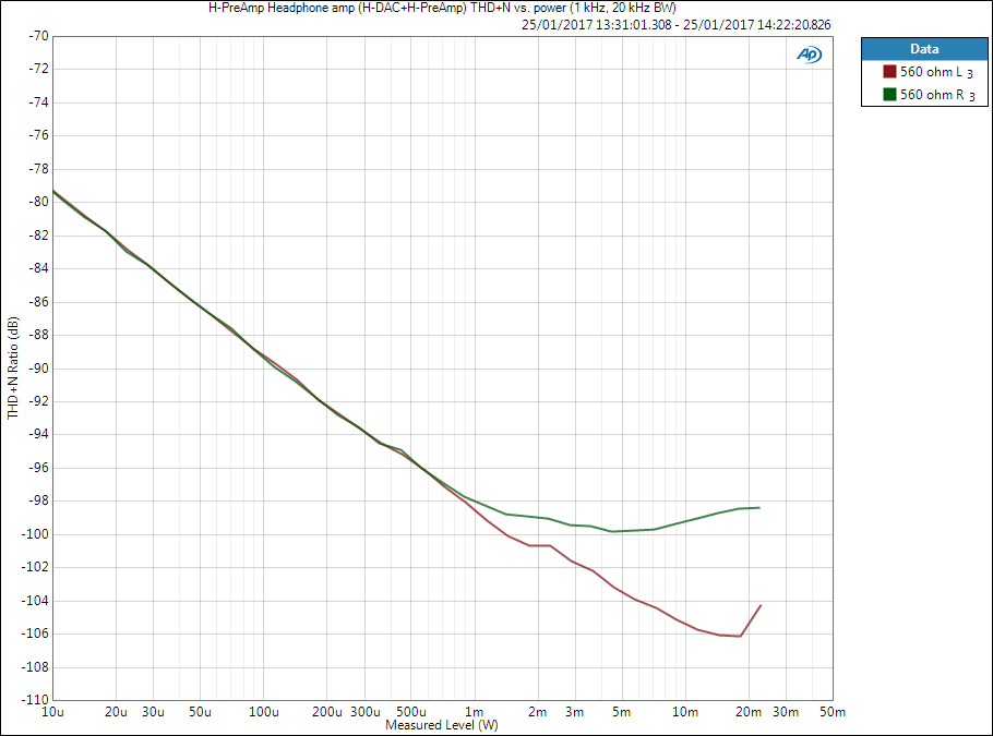
With 33 ohms the curve looks quite different. Distortion is higher but well under control. Would be interesting to understand the cause for the shape of the graph though. These are very high power levels for headphones. It is clear that the amplifier could give much more power – and by adding more gain you could do that. I am sure 200 mW is enough for me. Practical listening levels are probably closer to that 1-2 mW dip.
Crosstalk
Crosstalk in typical headphone systems is quite bad simply due to common ground point. Even the flat line across frequency tells that this coupling is not capacitive as typical crosstalk but something else. This is not a flaw of the amplifier IC or the circuit but the connection. With traditional 3.5 mm or 6.3 mm plugs there is a common ground connection for both channels. This causes significant crosstalk between channels. This coupling gets worse with low-impedance headphones as current is higher. This phenomenon can be avoided with separate headphone cabling for each channel but this requires modified cables/headphones. I will address that at a later time in another post and measurements.
Pops and clicks
I have not quantified pop and click performance but both line output and headphone amplifier show rather large clicks when the board is powered up and down. This is simply due to uncontrolled rise of supply voltages. This could cause issues in some systems. As a preamplifier it can be avoided by turning the power amplifier on after the preamp (which should be done anyway) but with headphones this can be a real issue without any mute function.
Files
- v1.0A
- Schematics
- Component placement top
- Component placement bottom
- c-file for HP Pre 2016 software
- BOM
- Check carefully before making component order
- Prices are in GBP, without VAT, and not up-to-date)
References
Version history
Schematics / PCB version history and known errors and bugs
- v1.0A Initial version
- Pinheaders (silkscreen) are on top side although they should be on bottom
- “MC” and “BC” wrong way on silkscreen
- For 2.0, remove THAT1606
- Consider output mute circuits for future versions
This page version history
- 25.1.2017 Initial version
2 comments
May I know what chip is used to generate negative 12v?
Nothing on this board. It is meant to be used with H-DAC which provides supplies via pinheaders. This board only generates +5V and -5V as those are not available on H-DAC.