
Easy and quick way to check new footprints, that you definitely read all datasheet measures correctly when drawing the footprint, is to print the layout on paper and fit components on it.
It is highly recommended to check new footprints before sending PCB files for manufacturing. I check all new footprints, whether I have created them myself or they are in the CAD tool library. Once I have used them, I can trust they are ok although it may still be good to check, especially if you use slightly different parts even if assuming package is the same. Obviously care should be taken when drawing new footprints, and datasheed used as guidelines, but check on paper print gives good confidence all is correct. Sometimes you may also prefer slightly different sized footprint than guided on datasheet, especially when hand-soldering.
Another useful point is to get a real sense of scale. Especially when working on small components on small boards, board, components, and clearances may look huge on screen but are actually tiny in practice. Maybe connectors, switches, or other user operated parts are too close to one another, or things should be moved slightly from EMC perspective.
If possible, it is also good to fit the PCB paper model on the enclosure to be.
Simple way to check components is to print the PCB design on paper and see how the components fit. Just ensure there is no scaling when printing from CAD tool and/or PDF.
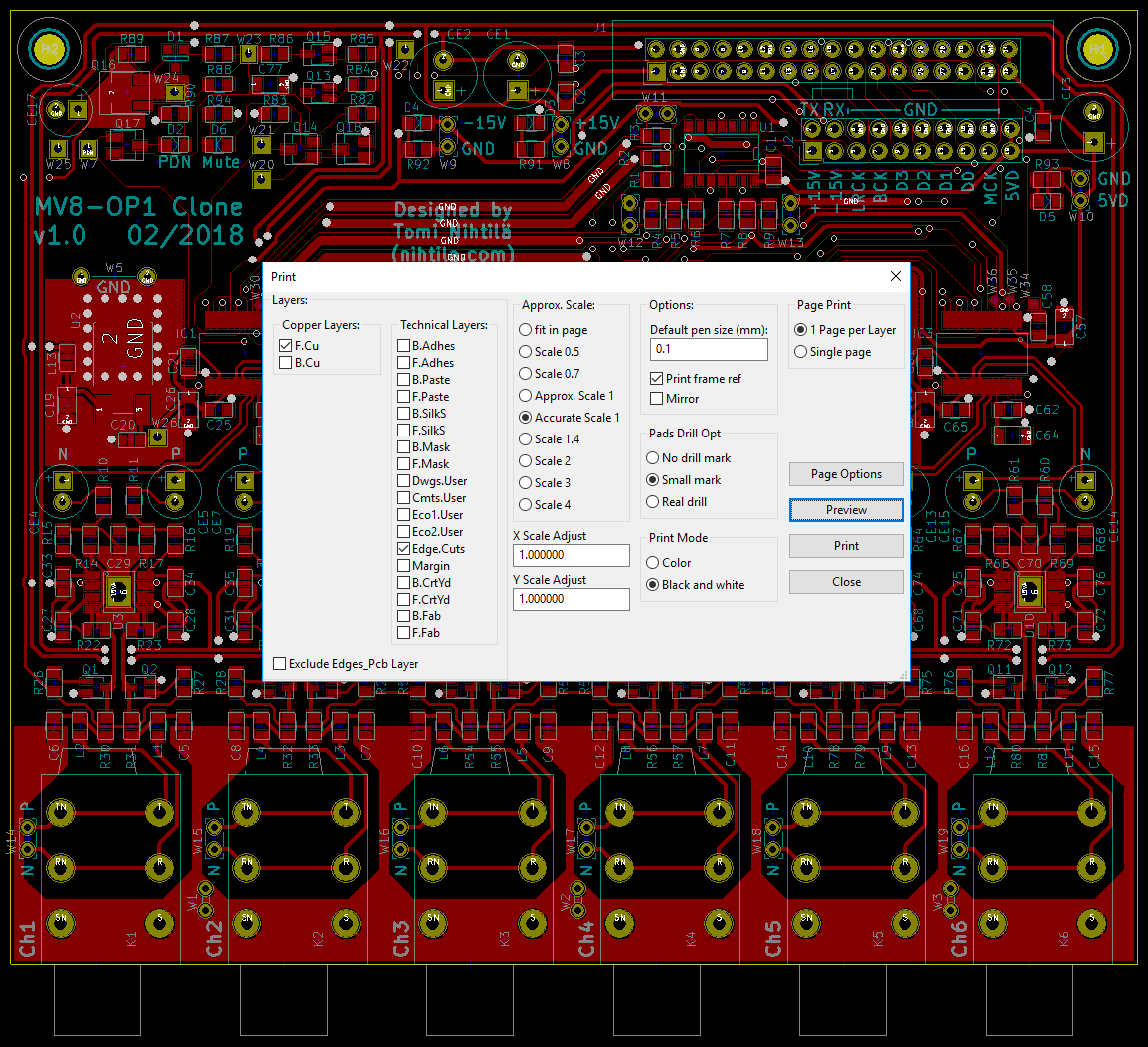
Choose accurate scale 1 when printing from KiCad
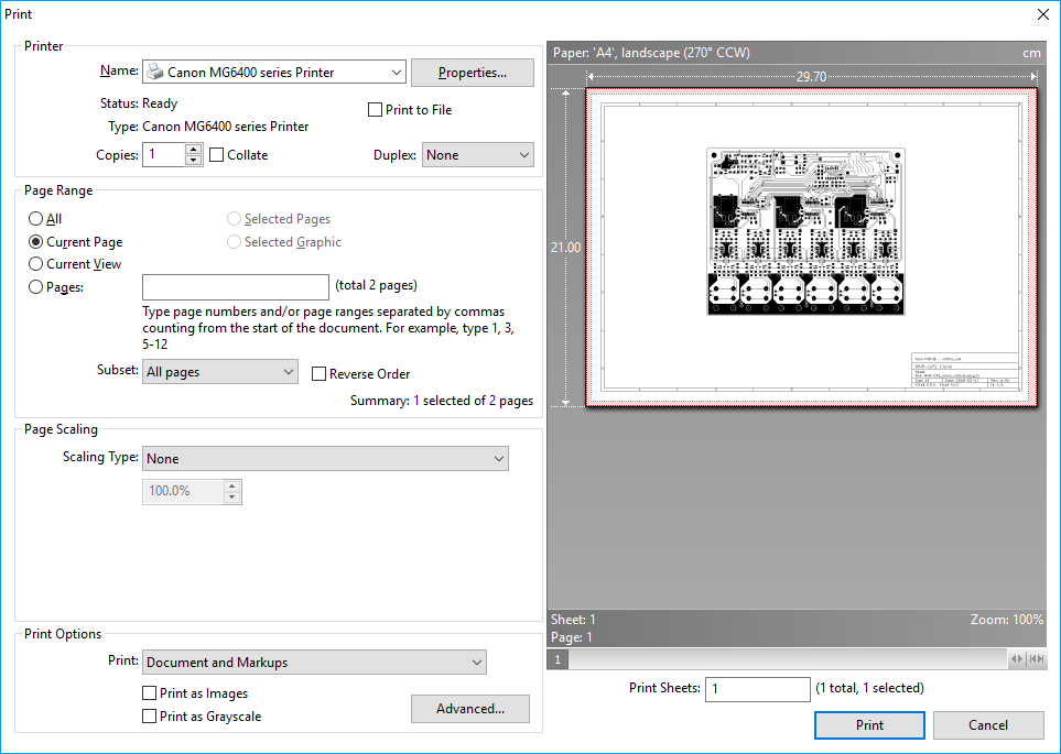
Choose no scaling when printing from PDF
After printing, ensure correct scale by measuring board outlines. Then just place the critical components on your print. Even if it is a decent fit, sometimes you may want to move or extend pads to provide more or less space for hand-soldering. For example my own generic 1206/0805/etc footprints on KiCad are somewhere between the provided factory-solder and hand-solder footprints.
2 comments
This is really good tip. While its simple. I never thought of this.
Thank you.
So, you know how you do this printing to check if the packages are correct? I did the same a while ago for the PCM2912A DAC I’m building…and found out that I made my PCB facing the wrong side in a 90º rotation. ♂️